

Field effect transistor with three-sag structure and preparation method thereof
A field-effect transistor, recessed structure technology, applied in semiconductor/solid-state device manufacturing, semiconductor devices, electrical components, etc., can solve the problem that the saturation leakage current is not substantially improved, the effective carrier mobility is reduced, and the drain current is reduced. and other problems, to achieve the effects of increased breakdown voltage, increased saturation leakage current, and reduced gate-to-drain capacitance
- Summary
- Abstract
- Description
- Claims
- Application Information
AI Technical Summary
Problems solved by technology
Method used
Image

Examples
Embodiment 1
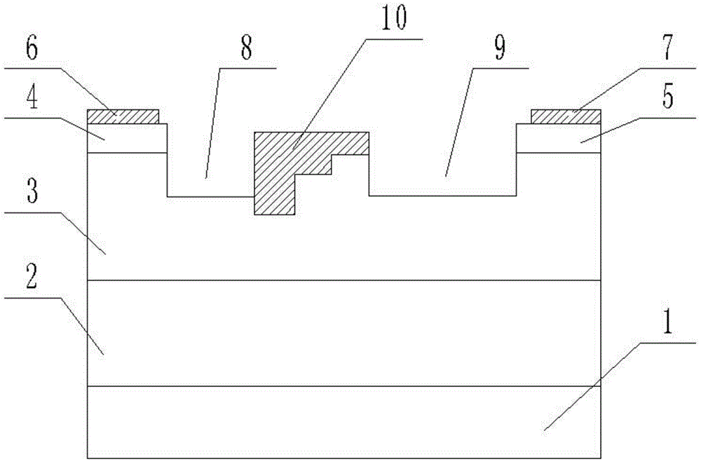
[0036] A field effect transistor with a three-recess structure with the lengths of the lower gate, the middle gate and the upper gate of the gate electrode 10 being 0.2 μm, 0.2 μm, and 0.3 μm respectively, and the step height being 0.05 μm was prepared.
[0037] Follow the steps below:
[0038] Step 1) cleaning the 4H-SiC semi-insulating substrate 1 to remove dirt on the surface of the substrate;
[0039] a. Carefully clean the substrate two or three times with a cotton ball dipped in methanol to remove SiC particles of various sizes on the surface;
[0040] b. Place 4H-SiC semi-insulating substrate 1 in H 2 SO 4 :HNO 3 = Ultrasound for 5 minutes in 1:1;
[0041] c. Put the 4H-SiC semi-insulating substrate 1 in 1# cleaning solution (NaOH:H 2 o 2 :H 2 O=1:2:5) and boiled for 5 minutes, then rinsed with deionized water for 5 minutes and then put into 2# cleaning solution (HCl:H 2 o 2 :H 2O=1:2:7) and boiled for 5 minutes, finally rinsed with deionized water and rinsed ...
Embodiment 2
[0075] A 4H-SiC metal-semiconductor field effect transistor with a three-recess structure with the low, middle, and high gate lengths of the gate electrode 10 being 0.2 μm, 0.3 μm, and 0.2 μm and a step height of 0.05 μm was fabricated. The difference between this embodiment and Embodiment 1 lies in step 7)
[0076] a. Use positive photoresist, coating speed: 3000R / min, glue thickness > 2μm to ensure the etching masking effect of the glue during subsequent etching;
[0077] b. After gluing, pre-bake in a 90°C oven for 90 seconds, use a concave groove photolithography plate for about 35 seconds of ultraviolet exposure, and then develop in a special developer for 60 seconds. The formula of the special developer: tetramethylammonium hydroxide: Water = 1:3, then post-bake in an oven at 100°C for 3 minutes;
[0078] c. Using ICP inductively coupled plasma etching system for N + Etching, the etching conditions are etching power 375W, bias power 60W, working pressure 9Pa, and the e...
Embodiment 3
[0082] Fabricate a 4H-SiC metal-semiconductor field-effect transistor with a three-recess structure with the low, middle, and high gate lengths of the gate electrode 10 being 0.3 μm, 0.2 μm, and 0.2 μm, respectively, and a step height of 0.05 μm. The difference between this embodiment and Embodiment 1 lies in step 7)
[0083] a. Use positive photoresist, coating speed: 3000R / min, glue thickness > 2μm to ensure the etching masking effect of the glue during subsequent etching;
[0084] b. After gluing, pre-bake in a 90°C oven for 90 seconds, use a concave groove photolithography plate for about 35 seconds of ultraviolet exposure, and then develop in a special developer for 60 seconds. The formula of the special developer: tetramethylammonium hydroxide: Water = 1:3, then post-bake in an oven at 100°C for 3 minutes;
[0085] c. Using ICP inductively coupled plasma etching system for N + Etching, the etching conditions are etching power 375W, bias power 60W, working pressure 9Pa,...
PUM
| Property | Measurement | Unit |
|---|---|---|
| Length | aaaaa | aaaaa |
| Length | aaaaa | aaaaa |
| Length | aaaaa | aaaaa |
Abstract
Description
Claims
Application Information