

Fabricating method of 3D magnetic sensor
A technology of a magnetic sensor and a manufacturing method, which is applied in the manufacturing/processing of electromagnetic devices, instruments, measuring magnetic variables, etc., can solve problems such as affecting the process, device dirty spots, contamination of the machine, etc., and achieves a slight and reduced sputtering accumulation phenomenon. The effect of roughness
- Summary
- Abstract
- Description
- Claims
- Application Information
AI Technical Summary
Problems solved by technology
Method used
Image

Examples
Embodiment 1
[0044] Please refer to Figure 5 , and combined with Figures 6 to 11 , the present invention provides a kind of manufacturing method of 3D magnetic sensor, comprises the following steps:
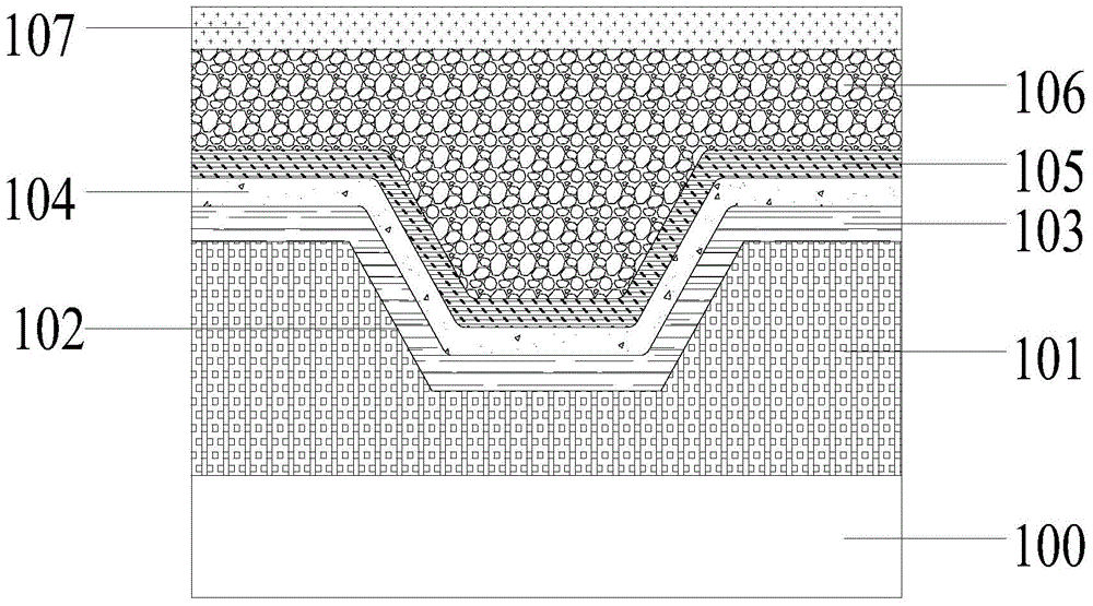
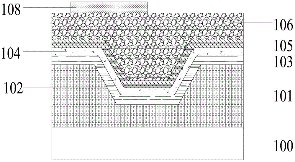
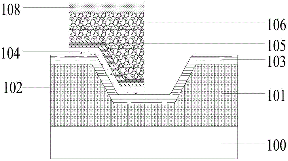
[0045] Please refer to Figure 6 , provide a substrate 300, deposit an insulating layer 302 on the substrate 300, and make a trench 301 in the insulating layer 302, the depth of the trench 301 is smaller than the thickness of the insulating layer 302, that is to say, the bottom of the trench 301 Instead of the upper surface of the substrate 300, the trenches 301 provide sidewalls for forming the magnetoresistive layer of the 3D magnetic sensor.
[0046] Preferably, the material of the substrate 300 is silicon, germanium, or a layer of silicon covered on an insulator as the substrate.
[0047] The way to form the trench 301 is: use thermal oxidation growth or chemical vapor deposition process to form an insulating layer 302 on the substrate 300, cover the insulating layer 302 with a photo...
Embodiment 2
[0066] The difference between this embodiment and the first embodiment is that before depositing the magnetic material layer 303 , a diffusion barrier layer is deposited, and the diffusion barrier layer covers the insulating layer 302 and the bottom and sidewalls of the trench 301 .
[0067] Specifically, the material of the diffusion barrier layer is silicon nitride, and the formation method is chemical vapor deposition. The diffusion barrier layer can prevent the elements in the magnetic material layer 303 from diffusing into the insulating layer 302, especially metal ions, and avoid the insulation of the insulating layer 302. The effect is invalid.
PUM
 Abstract
Description
Claims
Application Information