Full-laser grooving and scribing method of large-area copper indium gallium selenide (CIGS) thin-film solar cell assembly

一种太阳能电池、铜铟镓硒的技术,应用在电气元件、电路、光伏发电等方向,能够解决易发生翻边和崩边、加大组件制造成本、组件功率损失等问题,达到提高生产效率、降低生产和维护成本、提高组件功率的效果

Active Publication Date: 2015-10-21
BEIJING SIFANG JIBAO AUTOMATION
View PDF3 Cites 29 Cited by
  • Summary
  • Abstract
  • Description
  • Claims
  • Application Information

AI Technical Summary

Problems solved by technology

At present, for the production of large-area copper-indium-gallium-selenium thin-film solar cell modules, mechanical needles are generally used in the industry to scribe. Flanging and edge collapse occur, the dead zone width can reach more than 500 μm to 600 μm, and the power loss of the module is high; at the same time, the loss of the mechanical needle is serious, requiring frequent replacement of the mechanical needle and regular maintenance of the equipment, which increases the manufacturing cost of the module

Method used


Image

  • Full-laser grooving and scribing method of large-area copper indium gallium selenide (CIGS) thin-film solar cell assembly
  • Full-laser grooving and scribing method of large-area copper indium gallium selenide (CIGS) thin-film solar cell assembly
  • Full-laser grooving and scribing method of large-area copper indium gallium selenide (CIGS) thin-film solar cell assembly

Examples


Embodiment 1

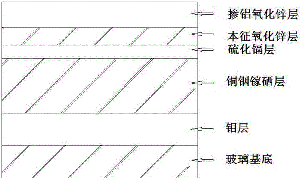
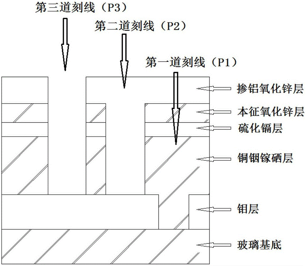
[0031] figure 1 It is a structural schematic diagram of a large-area copper indium gallium selenium thin film solar cell described in the present invention; as figure 1 As shown, the battery includes a glass substrate, a molybdenum layer, a copper indium gallium selenide layer, a cadmium sulfide layer, an intrinsic zinc oxide layer and an aluminum-doped zinc oxide layer; figure 2 It is a structural schematic diagram of full laser scribing of a large-area copper indium gallium selenium thin film solar cell according to the present invention; as figure 2 As shown, the all-laser scribing method includes three laser scribing. First, a molybdenum film is prepared on a glass substrate, and a laser is used to cut the prepared molybdenum film to form the first scribe line (P1); On the molybdenum layer scored by P1, the following film layers are prepared in sequence: copper indium gallium selenide film, cadmium sulfide film, and intrinsic zinc oxide film. Laser 2 is used to scribe t...

Embodiment 2

[0042] Step 1 is the same as in Example 1.

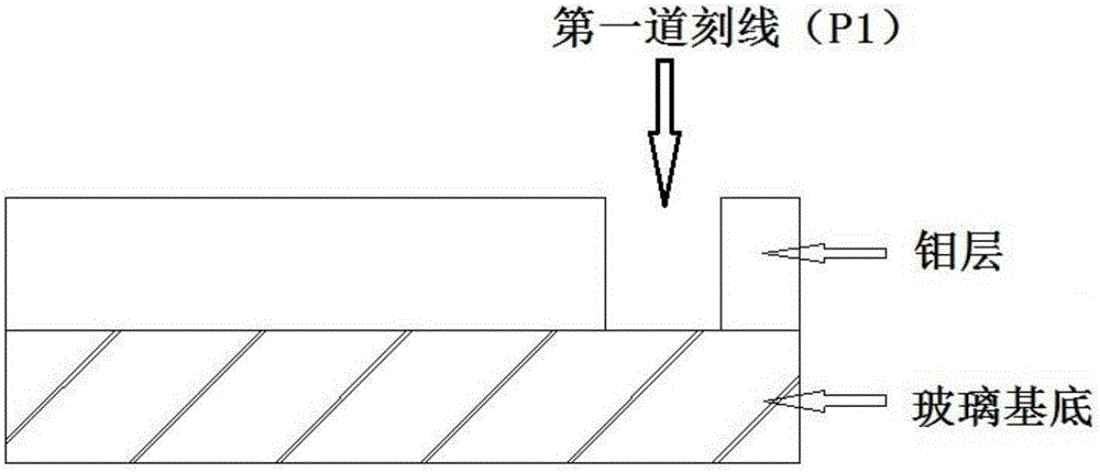
[0043] Step 2, P1 scribing: use a picosecond laser with a pulse width of 8 picoseconds, a wavelength of 532nm, a scribing power of 2.5W, a single pulse energy of 31.25μJ, and a repetition rate of 80kHz. The laser is incident from the back of the coating substrate, and the sample is Carry out P1 scribing, and the scribing speed is 2m / s. After scribing, the width of the scribed line is 35 μm, and the Mo layer in the scribed line is completely removed, exposing the surface of the soda-lime glass.

[0044] Step 3 to step 8 are the same as in Example 1.

Embodiment 3

[0046] Step 1 is the same as in Example 1.

[0047] Step 2, P1 scoring: use a nanosecond laser with a pulse width of 10 nanoseconds, a wavelength of 1064nm, a scoring power of 3.2W, a single pulse energy of 40uJ, and a repetition rate of 80kHz. The laser is incident from the back of the coating substrate, and the sample is processed For P1 marking, the marking speed is 2m / s. After scribing, the width of the scribed line is 33 μm, and the Mo layer in the scribed line is completely removed, exposing the surface of the soda-lime glass.

[0048] Step 3 to step 8 are the same as in Example 1.


PUM

PropertyMeasurementUnit
energyaaaaaaaaaa
poweraaaaaaaaaa
energyaaaaaaaaaa

Abstract

The invention provides a full-laser grooving and scribing method of a large-area copper indium gallium selenide (CIGS) thin-film solar cell assembly. The method comprises steps of using a laser to groove and scribe a molybdenum thin film prepared on soda-lime glass so as to form a first scribed line (P1); successively preparing a CIGS layer, a cadmium sulfide layer and an intrinsic zinc oxide layer on the molybdenum layer where the P1 has been grooved and scribed; after finishing the above film layer preparation, using a laser to perform grooving and scribing so as to form a second scribed line (P2) which is parallel to the P1; and after preparing an aluminum-doped zinc oxide layer on the intrinsic zinc oxide layer where the P2 has been grooved and scribed, using a laser to perform grooving and scribing so as to form a third scribed line (P3) which is parallel to the P1. According to the invention, inner join is performed for the CIGS thin-film solar cell assembly by the laser grooving and scribing method, so defects of large area of dead zones and frequency change of machinery needles in traditional machinery grooving and scribing technology can be overcome, thereby increasing efficiency of the assembly, improving stability of the grooving and scribing device and achieving objectives to reduce production cost and improve production efficiency.

Description

technical field [0001] The invention belongs to the technical field of thin-film solar cells, and in particular relates to a method for manufacturing large-area copper indium gallium selenium thin film solar cell components. Background technique [0002] Energy crisis and environmental pollution are two basic problems facing the world today. Solar energy is inexhaustible and inexhaustible, which is an important way to solve the energy crisis. Copper indium gallium selenide thin film solar cells have become one of the most promising photovoltaic materials in thin film solar cells because of their adjustable optical bandgap, strong radiation resistance, stable battery performance, and good low-light performance. [0003] Cell interconnection technology is one of the key technologies for the production of CIGS thin film solar modules. At present, for the production of large-area copper-indium-gallium-selenium thin-film solar cell modules, mechanical needles are generally used...

Claims


Application Information

Patent Timeline
Patent Type & Authority Applications(China)
IPC IPC(8): H01L31/18H01L21/78
CPCH01L31/18H01L31/0749H01L31/0463Y02E10/541Y02P70/50H01L21/78H01L31/022425H01L31/022483H01L31/0392H01L31/186H01L31/1884H01L31/046
Inventor 张宁余新平戴万雷
Owner BEIJING SIFANG JIBAO AUTOMATION
Why Eureka
Try Eureka