Preparation method for semiconductor power device structure, and structure

A technology of power devices and semiconductors, applied in the direction of semiconductor devices, semiconductor/solid-state device manufacturing, transistors, etc., can solve the problems of long turn-off time of devices and affect the high-frequency performance of devices, so as to improve device performance, reduce on-resistance, The effect of increasing the effective concentration

Active Publication Date: 2015-11-18
工业和信息化部电子第五研究所华东分所
View PDF4 Cites 4 Cited by
  • Summary
  • Abstract
  • Description
  • Claims
  • Application Information

AI Technical Summary

Problems solved by technology

However, when the device is turned on, there are a large number of holes in the drift region. When the device is turned off, the recombination and extraction of minority carriers takes a certain amount of time, that is, the so-called minority carrier storage effect, which will form a so-called "tailing current". Makes the off-time of the device longer and affects the high-frequency performance of the device

Method used


Image

  • Preparation method for semiconductor power device structure, and structure
  • Preparation method for semiconductor power device structure, and structure
  • Preparation method for semiconductor power device structure, and structure

Examples


Embodiment 1

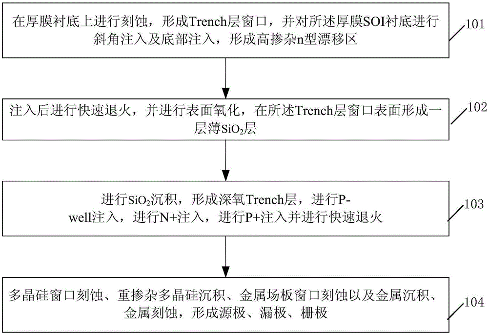
[0028] refer to figure 1 , figure 1 It is a schematic flow chart of a method for preparing a semiconductor power device structure according to an embodiment of the present invention.

[0029] In Embodiment 1, the preparation method of the semiconductor power device structure includes:

[0030] Step 101, performing etching on the thick-film SOI substrate to form a Trench layer window, and performing oblique angle implantation and bottom implantation on the thick-film SOI substrate to form a highly doped n-type drift region;

[0031] Step 102, perform rapid annealing after implantation, and perform surface oxidation to form a thin layer of SiO on the surface of the Trench layer window 2 layer;

[0032] Step 103, carry out SiO 2 Deposition, formation of deep oxygen trench layer, P-well implantation, N+ implantation, P+ implantation and rapid annealing;

[0033] Step 104, polysilicon window etching, heavily doped polysilicon deposition, metal field plate window etching, metal...

Embodiment 2

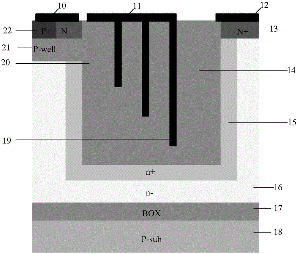
[0050] refer to figure 2 , figure 2 It is a schematic diagram of the structure of the semiconductor power device of the embodiment of the present invention.

[0051] In Embodiment 2, the semiconductor power device structure includes:

[0052] Source, source metal, gate metal, drain, drain metal, source body region, polysilicon, metal field plate, N-type heavily doped region, oxygen Trench layer, N-type drift region, buried oxide layer, P-type lining end;

[0053] The P-type substrate is on the bottom layer of the semiconductor power device structure, the buried oxide layer is on the P-type substrate, the N-type drift region is on the buried oxide layer, and the N-type The heavily doped region is above the N-type drift region, the oxygen Trench layer is above the N-type heavily doped region, and the metal field plate is a vertical field plate with multiple layers of different lengths. A heavily doped n-type layer is injected into the N-type drift region near the surface o...

Embodiment 3

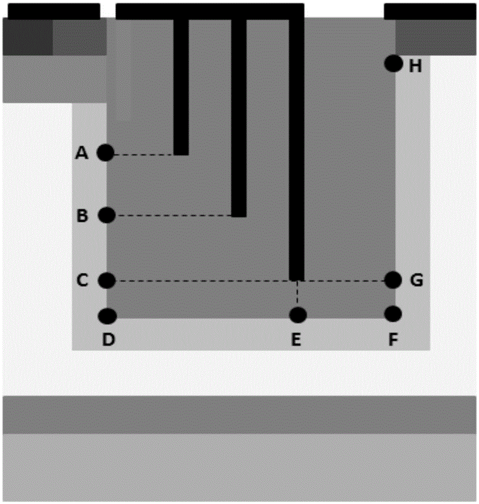
[0058] refer to image 3 , image 3 It is another schematic diagram of the structure of the semiconductor power device of the embodiment of the present invention.

[0059] Figure 4 It is a schematic diagram of the electric field of a semiconductor power device according to an embodiment of the present invention.

[0060] Specifically, the breakdown voltage of the LDMOS structure of a lateral power device is determined by both the lateral withstand voltage and the vertical withstand voltage, and within a certain range, the lateral withstand voltage of the device is proportional to the length of the drift region and inversely proportional to the doping concentration of the drift region , while the on-resistance of the device is just the opposite. Therefore, there is a contradictory relationship between the breakdown voltage and the on-resistance of the lateral power device.


PUM


Abstract

The embodiment of the invention discloses a preparation method for a semiconductor power device structure, and a structure. A Trench layer of a conventional lateral power device Trench LDMOS structure is provided with a plurality of longitudinal metal field plates at different depths, and a drift region is provided with a heavily-doped n-type layer. In order to improve the breakdown voltage of a device, the metal field plates with different lengths at different layers can introduce a plurality of new electric field peak values in a drift region, and enables a surface high electric field to be introduced into a body, thereby protecting the surface of the device from being broken down in advance. After complete loss, the heavily-doped n-type layer improves the surface charge density of the Trench layer, improves the electric fields of the Trench layer and the drift region, and improves the breakdown voltage of the device. In order to reduce the conduction resistance of the device, a deep oxygen Trench layer reduces the length of the lateral drift region.

Description

technical field [0001] Embodiments of the present invention relate to the technical field of semiconductors, and in particular to a method and structure for preparing a semiconductor power device structure. Background technique [0002] Power integrated circuits are sometimes called high-voltage integrated circuits, which are an important branch of modern electronics. They can provide new circuits with high speed, high integration, low power consumption and radiation resistance for various power conversion and energy processing devices, and are widely used in electric power Daily consumption fields such as control systems, automotive electronics, display device drivers, communications and lighting, as well as many important fields such as national defense and aerospace. The rapid expansion of its application scope has also put forward higher requirements for the high-voltage devices in its core part. [0003] For the power device MOSFET, under the premise of ensuring the br...

Claims


Application Information

Patent Timeline
Patent Type & Authority Applications(China)
IPC IPC(8): H01L29/78H01L29/06H01L29/40H01L21/336
CPCH01L29/0611H01L29/404H01L29/407H01L29/66568H01L29/7825H01L29/0878H01L29/7824
Inventor 夏超张琦
Owner 工业和信息化部电子第五研究所华东分所
Why Eureka
Try Eureka