Communication and lighting multiplex LED lamp

A technology of LED lamps and substrates, applied in lighting devices, fixed lighting devices, lighting and heating equipment, etc., can solve the problems of LED luminous efficiency attenuation, phosphor quantum efficiency reduction, etc., to achieve simple production, improve service life and luminescence Efficiency, the effect of simplifying the packaging process

Inactive Publication Date: 2015-11-25
NANJING UNIV OF POSTS & TELECOMM
View PDF4 Cites 8 Cited by
  • Summary
  • Abstract
  • Description
  • Claims
  • Application Information

AI Technical Summary

Problems solved by technology

However, as the lighting time of the LED chip increases, the temperature of the chip rises, and the heat generated by the chip is transferred to the phosphor and the fluorescent glue, resulting in a gradual decrease in the quantum efficiency of the phosphor, which makes the LED luminous efficiency attenuate.

Method used


Image

  • Communication and lighting multiplex LED lamp
  • Communication and lighting multiplex LED lamp
  • Communication and lighting multiplex LED lamp

Examples


preparation example Construction

[0027] a. Preparation of fluorescent vitreous body

[0028] The content of the rare earth element doped in the luminescence center is 0-10 mol%, the content of the glass matrix is ​​100-90 mol%, and the mass sum of the above components is 100 mol%. Among them, the luminescent center is one or more rare earth ions (Dy 3+ 、Sm 3+ , Tb 3+ 、Eu 3+ 、Eu 2+ 、Ce 2+ 、Tm 3+ 、Ho 3+ etc.) and transition metal ions (Mn 2+ , Sn 4+ etc.); glass substrates include silicates, phosphates, borates, tellurates, etc. It is mainly prepared by high temperature melting method.

[0029] b. Preparation of fluorescent ceramic body

[0030] The amount of fluorescent micro-nano crystals doped with the luminescent center is 1-60 mol%, the glass matrix is ​​40-99 mol%, and the sum of the above components is 100 mol%. Among them, fluorescent micro-nano crystals are uniaxial crystals of cubic crystal phase (such as Y 2 o 3 , YAG, etc.), the luminescent center is one or more rare earth ions (Dy 3+...

Embodiment 1

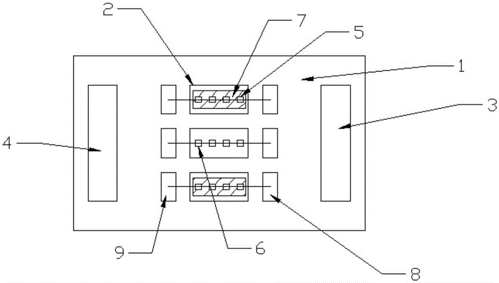
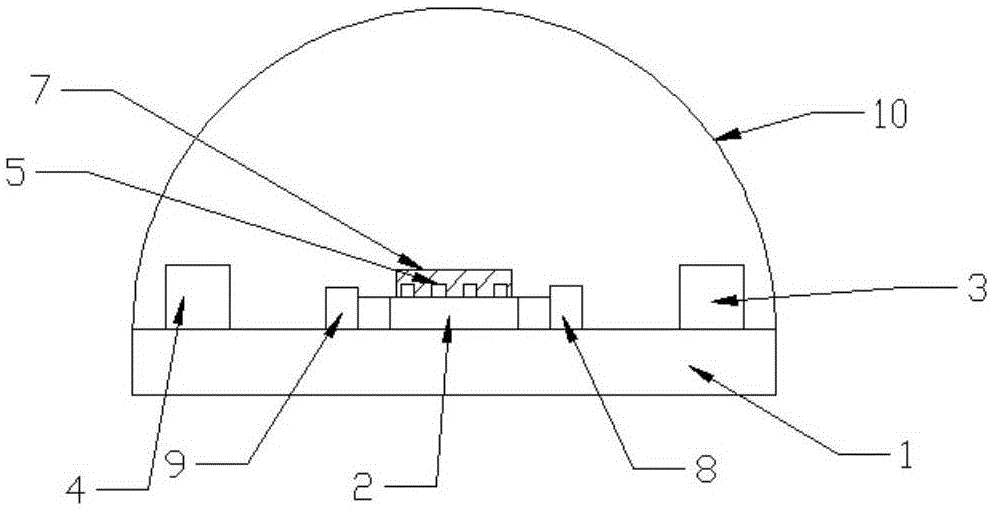
[0037] First, a transparent ceramic phosphor is prepared. The co-precipitation method was used to synthesize YAG:Ce fluorescent micro-nano crystals, the particle size of which was about 30-50nm. Weigh 20g of YAG:Ce fluorescent micro-nano crystals for later use. Then, 30 g of tellurite glass powder was prepared by high-temperature melting method, and the refractive index and dispersion of the glass were adjusted to match YAG:Ce by adjusting the ratio of glass components. The fluorescent micro-nano crystals and the glass matrix powder are mixed in proportion and placed in a crucible, and the glass matrix is ​​melted in a furnace, fully stirred and then quenched to obtain a transparent ceramic phosphor. Finally, light-emitting structures of various sizes and shapes are processed according to lighting requirements (below figure 1 The phosphor 7 in the figure is a transparent phosphor sheet processed through grinding, polishing and other processes).

[0038] Then, on the substra...

example 2

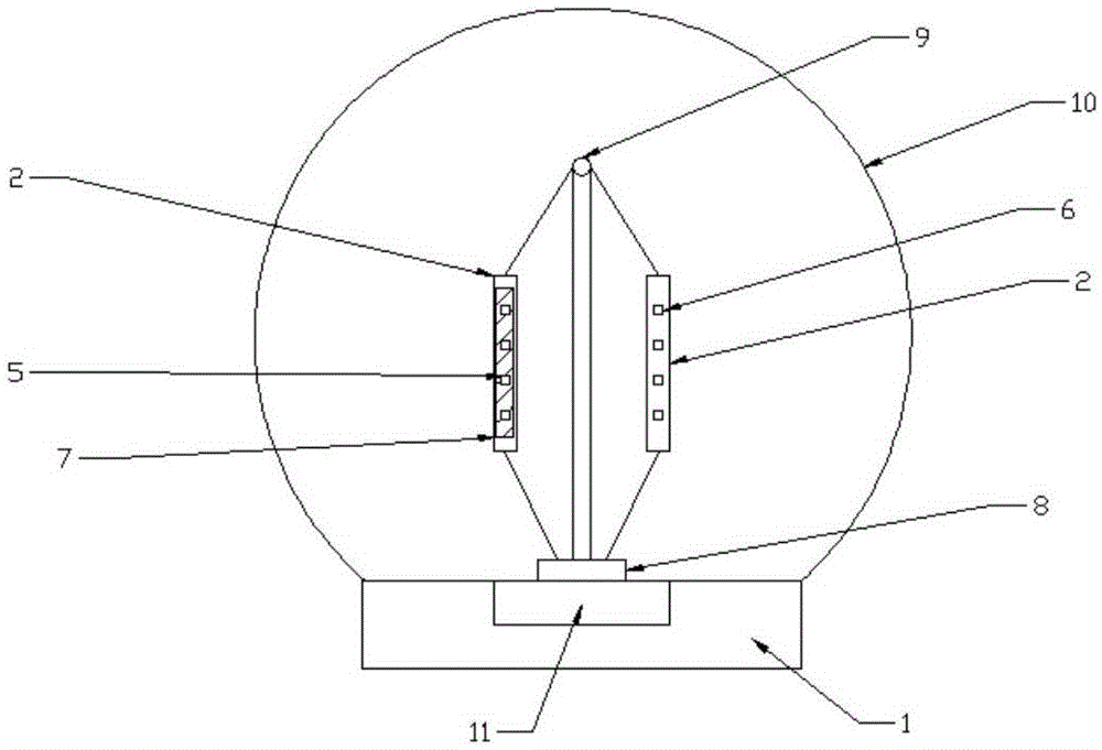
[0040] First, the glass phosphor is prepared by a high-temperature melting method. Raw material ratio is 41P 2 o 5 -17K 2 O-8Al 2 o 3 -20BaF 2 -3PbF 2 -10LiF-Dy 2 o 3 Weigh 25g of raw material, mix and shake well, and pour it into a 50ml quartz crucible; put the quartz crucible into a high-temperature furnace with a temperature of 1000°C and keep it warm for 1h; stir and shake well, then pour it into a 340°C copper mold to quench; put Annealed in a muffle furnace at 360°C for 5 hours. Finally, light-emitting structures of various sizes and shapes are processed according to lighting requirements (below image 3 The phosphor 7 in the figure is a transparent phosphor hollow tube that is post-processed through processes such as grinding, polishing, and tube extrusion).

[0041] Then, the substrate 2 is made into strips, so that chips can be inlaid on both sides of the substrate, thereby greatly improving resource utilization. Part of the substrate is used to inlay 360nm...


PUM


Abstract

The invention discloses a communication and lighting multiplex LED lamp. The LED lamp comprises two functions, wherein one of the functions is white-light lighting, and the other function is being used as a transmitting terminal of infrared communication. As to the function of lighting, one or more types of rare earth ions such as Dy3+, Sm3+, Tb3+, Eu3+, Eu2+, Ce2+, Tm3+, Ho3+ and the like and transition metal ions such as Mn2+, Sn4+ and the like are taken as an active luminescence center, glass or transparent glass ceramic is taken as a base material, and fluorescent light is excited to be emitted through an ultraviolet or a blue LED chip. The infrared communication transmitting terminal takes an infrared LED chip which is suitable for being used as a short-range wireless infrared communication channel (800nm-1000nm waveband) as a signal emission source, modulated pulses are loaded to a driving circuit of the infrared LED chip, then electric signals are converted into wireless optical signals, and transmission and delivery of information are carried out. The LED lamp disclosed by the invention has the advantages of low preparation cost, good stability, large modulation bandwidth, high modulation power, long service life and small size.

Description

technical field [0001] The invention belongs to the field of LED and communication application thereof, and in particular relates to a visible light illumination and infrared light wireless communication system of LED and a device thereof. Background technique [0002] In recent years, along with the rapid development of semiconductor technology, visible light communication based on LED (Light Emitting Diode, Light Emitting Diode) lighting as a wireless access technology has also been rapidly developed. The advantage is that the existing LED device for lighting can be directly used to realize the unification of lighting and communication, so as to save resources and widen the communication spectrum. However, its communication system is not mature enough, the uplink and downlink communication protocols are difficult to unify, and the current working stability of LED lights still needs to be improved. Therefore, it is important to develop high compatibility and high stability ...

Claims


Application Information

Patent Timeline
Patent Type & Authority Applications(China)
IPC IPC(8): H01L33/52H01L33/50F21S8/00
CPCH01L33/56F21S8/00H01L33/505
Inventor 韦玮袁野郑锐林陈晓红
Owner NANJING UNIV OF POSTS & TELECOMM
Why Eureka
Try Eureka