Nanometer material transmission electron microscope in-situ testing chip, preparation method and applications thereof

A technique of transmission electron microscopy and in-situ testing, which is applied in the analysis of materials, metal material coating process, material analysis using wave/particle radiation, etc. , to achieve the effect of being suitable for mass production, simple production process and easy to promote

Active Publication Date: 2015-12-09
NANJING UNIV
View PDF4 Cites 29 Cited by
  • Summary
  • Abstract
  • Description
  • Claims
  • Application Information

AI Technical Summary

Problems solved by technology

However, the application of existing in-situ MEMS chips still has its limitations. Generally, only the Focused Ion Beam (FIB) system can be used for sample transfer and fixation, which limits the conditions of use and greatly increases the cost of use.
In addition, the focused ion beam system cannot avoid contamination of the sample during sample transfer and fixation, but the existing in-situ MEMS chip cannot process the sample after the transfer and fixation of the sample
The above limitations limit the application of in-situ MEMS chips to a large extent, and there is currently no good solution

Method used


Image

  • Nanometer material transmission electron microscope in-situ testing chip, preparation method and applications thereof
  • Nanometer material transmission electron microscope in-situ testing chip, preparation method and applications thereof
  • Nanometer material transmission electron microscope in-situ testing chip, preparation method and applications thereof

Examples


Embodiment 1

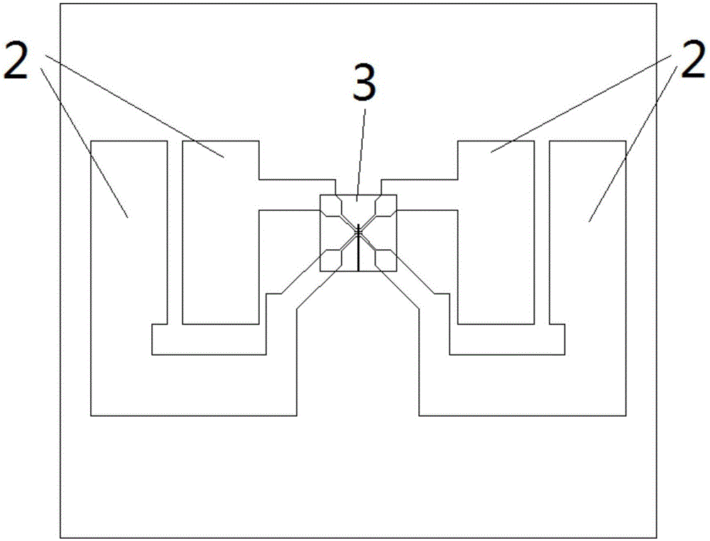
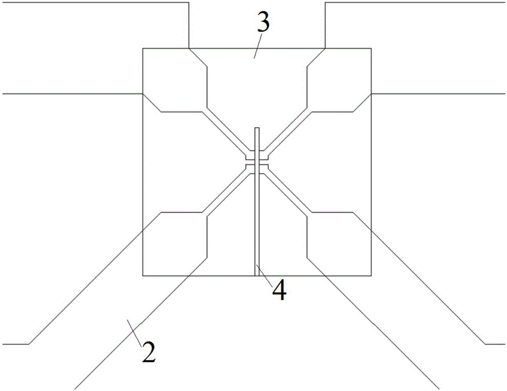
[0035] see figure 1 , figure 2 and image 3 , a nanomaterial transmission electron microscope in-situ electrical test chip of this embodiment, including a silicon substrate, an insulating layer, a thin film window 3 and an electron beam transmission region 4 . Specifically: the silicon substrate is a rectangular sheet with a thickness of 400 μm, and there are insulating layers on both sides of the silicon substrate, and the insulating layer includes a silicon dioxide layer grown on the silicon substrate and a silicon dioxide layer on the silicon dioxide layer. For the grown silicon nitride layer, the thickness of the silicon dioxide layer is 900nm, and the thickness of the silicon nitride layer is 200nm. On the insulating layer on the front side of the silicon substrate, metal thin films or devices that can apply various physical and chemical effects to the samples, or semiconductor functional thin films or devices, see figure 1 In this embodiment, a metal electrode 2 is f...

Embodiment 2

[0061] A nanomaterial transmission electron microscope in-situ electrical test chip and its preparation method in this embodiment are basically the same as in Embodiment 1, except that the thickness of the silicon substrate in this embodiment is 300 μm, and the metal electrodes are located on the film window. Some are distributed along one side of the electron beam-transmitting long groove, the length of the electron-beam transmitting long groove is 300 μm, and the width is 10 μm. The thickness of the metal electrode is 50nm, the thickness of the silicon dioxide layer in the insulating layer is 200nm, and the thickness of the silicon nitride layer is 5nm.

[0062] In this embodiment, the process of using the in-situ electrical test chip to transfer the nanowire sample in the laboratory using a micromanipulator (micromanipulator) is as follows:

[0063] (1) Under an optical microscope, a nanowire sample with a length of about 20 microns is picked up with the tip of a micromanip...

Embodiment 3

[0069] A nanomaterial transmission electron microscope in-situ electrical test chip and its preparation method in this embodiment are basically the same as in Embodiment 1, except that the thickness of the silicon substrate in this embodiment is 200 μm, and the metal electrodes are located on the film window. Parts are distributed along both sides of the electron beam-transmitting long groove, the length of the electron-beam transmitting long groove is 320 μm, and the width is 8 μm. The thickness of the metal electrode is 200nm, the thickness of the silicon dioxide layer in the insulating layer is 1000nm, and the thickness of the silicon nitride layer is 150nm.


PUM

PropertyMeasurementUnit
thicknessaaaaaaaaaa
thicknessaaaaaaaaaa
thicknessaaaaaaaaaa

Abstract

The present invention discloses a nanometer material transmission electron microscope in-situ testing chip, a preparation method and applications thereof, and belongs to the technical field of nanometer material performance in-situ testing. The chip comprises a silicon substrate, insulating layers and a film window, wherein the insulating layer respectively grows on both surfaces of the silicon substrate, a metal film or device or a semiconductor function film or device grows on the chip front surface insulating layer so as to apply various physical and chemical effects on a sample, the center of the chip is provided with the film window, and the film window region is provided with a electron beam penetrating long hole or electron beam penetrating long groove having a large aspect ratio. According to the present invention, the transmission electron microscope sample can be subjected to in-situ measurement under the atomic scale resolution, the nano-wire samples and the nano-tube samples can be subjected to in-situ characterization, the bulk samples and the heterojunction interface samples can be subjected to in-situ characterization, the placement of the sample through the micro manipulator in the focused ion beam system and the laboratory can be achieved, and the sample transferred and fixed on the chip can be continuously processed by using the ion reduction equipment.

Description

technical field [0001] The invention relates to the technical field of in-situ testing of nanomaterial properties, more specifically, to a nanomaterial transmission electron microscope in-situ testing chip, a chip preparation method and an application thereof. Background technique [0002] In recent years, nanomaterials have attracted widespread attention in the field of scientific research due to their nanoscale properties such as small size effects, surface effects, quantum size effects, and macroscopic quantum tunneling effects. Transmission Electron Microscope (TEM) is a powerful modern material characterization method, which is used to analyze the fine structure smaller than 0.2 μm that cannot be seen clearly under the optical microscope. Today's TEM is capable of sub-Angstrom resolution and is a powerful tool for analyzing nanomaterials. Nanomaterials have peculiar effects in the fields of electricity, heat, and mechanics. With the development of microelectromechanica...

Claims


Application Information

Patent Timeline
Patent Type & Authority Applications(China)
IPC IPC(8): G01N23/00H01J37/20B81C1/00B81B7/02
Inventor 王鹏蔡嵩骅古宸溢王双宝
Owner NANJING UNIV
Why Eureka
Try Eureka