Al component gradually-changed N-type LED structure and preparation method thereof

A LED structure and component gradual change technology, which is applied in the direction of electrical components, circuits, semiconductor devices, etc., can solve the problems of no application, etc., and achieve the effects of improving surface roughness, increasing electron concentration, and enhancing current expansion ability

Active Publication Date: 2015-12-09
SHANDONG INSPUR HUAGUANG OPTOELECTRONICS
View PDF9 Cites 15 Cited by
  • Summary
  • Abstract
  • Description
  • Claims
  • Application Information

AI Technical Summary

Problems solved by technology

[0010] The existing aluminum composition gradient is usually applied in the preparation of the buffer layer, but not in the preparation of the N-type region

Method used


Image

  • Al component gradually-changed N-type LED structure and preparation method thereof

Examples


Embodiment 1

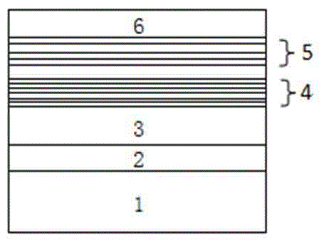
[0036] Such as figure 1 , taking the preparation of an N-type GaN structure on a silicon carbide substrate by metal-organic chemical vapor deposition as an example, which specifically includes the following steps:

[0037] (1) The silicon carbide substrate 1 is placed in the reaction chamber of the metal organic chemical vapor deposition furnace (MOCVD) equipment, heated to 800° C. under a hydrogen atmosphere, and processed for 15 minutes;

[0038] (2) growing an aluminum nitride nucleation layer 2 on a silicon carbide substrate 1 at a growth temperature of 450° C. and a thickness of 60 nm;

[0039] (3) growing a non-doped gallium nitride layer buffer layer 3 on the aluminum nitride nucleation layer 2, the growth temperature is 1150° C., and the growth thickness is 50 nm;

[0040] (4) N-type Al is grown on the gallium nitride buffer layer 3 Y In X Ga 1‐X‐Y For the N layer 4, set the growth temperature to 750° C., the growth pressure to 800 torr, and the growth time to 200 ...

Embodiment 2

[0044] Such as figure 1 , taking the preparation of an LED structure on a sapphire substrate by metal-organic chemical vapor deposition as an example, which specifically includes the following steps:

[0045] (1) The sapphire substrate 1 is placed in the reaction chamber of a metal organic chemical vapor deposition furnace (MOCVD), heated to 1300° C. under a hydrogen atmosphere, and processed for 5 minutes;

[0046] (2) growing an AlGaN nucleation layer 2 on a sapphire substrate 1 at a growth temperature of 650° C. and a thickness of 10 nm;

[0047] (3) growing a non-doped GaN layer buffer layer 3 on the AlGaN nucleation layer 2, the growth temperature is 800°C, and the growth thickness is 2000nm;

[0048] (4) N-type Al is grown on the gallium nitride buffer layer 3 Y In X Ga 1‐X‐Y For the N layer 4, set the growth temperature to 1600° C., the growth pressure to 200 torr, and the growth time to 3000 s. When growing, turn on the required silane for 1500s, and the silicon d...

Embodiment 3

[0053] Such as figure 1 , taking the preparation of an N-type superlattice structure on a sapphire substrate by metal-organic chemical vapor deposition as an example, which specifically includes the following steps:

[0054] (1) The sapphire substrate 1 is placed in the reaction chamber of a metal organic chemical vapor deposition furnace (MOCVD), heated to 1000° C. under a hydrogen atmosphere, and processed for 10 minutes;

[0055] (2) growing a gallium nitride nucleation layer 2 on a sapphire substrate 1 at a growth temperature of 550° C. and a thickness of 30 nm;

[0056] (3) growing a non-doped gallium nitride layer buffer layer 3 on the gallium nitride nucleation layer 2, the growth temperature is 1080°C, and the growth thickness is 1000nm;

[0057] (4) N-type Al is grown on the gallium nitride buffer layer 3 Y In X Ga 1‐X‐Y For the N layer 4, set the growth temperature to 1005° C., the growth pressure to 500 torr, and the growth time to 1500 s. When growing, turn on...


PUM

PropertyMeasurementUnit
thicknessaaaaaaaaaa
thicknessaaaaaaaaaa
thicknessaaaaaaaaaa

Abstract

An Al component gradually-changed N-type LED structure and a preparation method thereof are disclosed. The Al component gradually-changed N-type LED structure successively comprises, from bottom to top, a substrate, a nucleating layer, a buffer layer, an N-type Al<Y>In<X>Ga<1-X-Y>N layer, a multi-quantum well light-emitting layer, and a P-type GaN layer. In the N-type Al<Y>In<X>Ga<1-X-Y>N layer, X is more than or equal to 0 but less than or equal to 1, and Y is more than 0 but less than 1. An Al component in an N-type GaN layer is gradually changed. The method comprises the following steps of: (1) growing the nucleating layer on a processed substrate; (2) growing a non-doped gallium nitride buffer layer on the nucleating layer; (3) growing the N-type Al<Y>In<X>Ga<1-X-Y>N layer on the buffer layer; (4) growing the multi-quantum well light-emitting layer on the N-type Al<Y>In<X>Ga<1-X-Y>N layer, wherein the multi-quantum well light-emitting layer is formed by periodically and alternately superposed InGaN potential well layers and GaN barrier layers; and (5) growing the P-type GaN layer on the multi-quantum well light-emitting layer. An N-type region is prepared by an Al component gradually-changed mode, thereby improving electron concentration and an antistatic effect, essentially improving GaN film quality, enhancing current expansion capability, and increasing light extraction efficiency.

Description

technical field [0001] The invention relates to a structure and a preparation method of an N-type LED (light-emitting diode) with gradually changing Al components, and belongs to the technical field of LED (light-emitting diode) structures. Background technique [0002] In the early 1990s, the third-generation wide-bandgap semiconductor materials represented by nitrides made a historic breakthrough. Researchers successfully prepared blue-green and ultraviolet LEDs on gallium nitride materials, making LED lighting become possible. In 1971, the first gallium nitride LED die came out. In 1994, gallium nitride HEMTs appeared blue light GaN-based diodes with high electron mobility, and gallium nitride semiconductor materials developed very rapidly. [0003] Semiconductor light-emitting diodes have the advantages of small size, ruggedness, strong controllability of light-emitting bands, high luminous efficiency, low heat loss, low light decay, energy saving, and environmental pro...

Claims


Application Information

Patent Timeline
Patent Type & Authority Applications(China)
IPC IPC(8): H01L33/02H01L33/06H01L33/32H01L33/00
CPCH01L33/0075H01L33/02H01L33/06H01L33/32H01L33/325
Inventor 曲爽王成新逯瑶徐现刚
Owner SHANDONG INSPUR HUAGUANG OPTOELECTRONICS
Why Eureka
Try Eureka