Preparation method for implementing electron field emission device by use of graphene

A launch device and graphene technology, applied in the field of micro-electromechanical systems, can solve problems such as difficult industrialization, difficult process, expensive equipment, etc., and achieve low cost, avoid complex process, and environment-friendly effects

Inactive Publication Date: 2015-12-30
EAST CHINA NORMAL UNIV
View PDF7 Cites 6 Cited by
  • Summary
  • Abstract
  • Description
  • Claims
  • Application Information

AI Technical Summary

Problems solved by technology

Among these methods, the redox method and the metal surface growth method are mostly used. The graphene prepared by the redox method has a high yield and is suitable for large-scale production. However, the graphene prepared by this method has many defects and can only be used in supercapacitors. , lithium-ion batteries and other en

Method used


Image

  • Preparation method for implementing electron field emission device by use of graphene
  • Preparation method for implementing electron field emission device by use of graphene

Examples


Embodiment 1

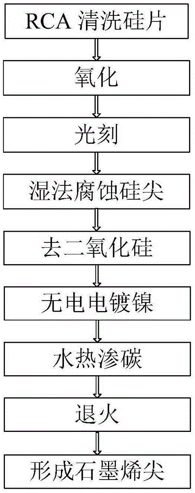
[0048] A preparation method of graphene electron field emission is as follows:

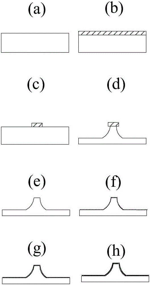
[0049] 1) Choose a 6-inch silicon wafer, n-type silicon with crystal orientation, resistivity 2-5Ω·cm, 500±50μm. The purpose of RCA cleaning solution is to remove particulate contamination (particles) and metal impurities. Liquid No.3 H 2 SO 4 (98% wt): H 2 o 2 (30%wt)=1:1 volume ratio mixing, remove organic contamination, soak for 15 minutes, rinse with hot and cold deionized water for 5 minutes each; No. 2 liquid NH 4 OH (28% wt): H 2 o 2 (30% wt): H 2 : O = 1:2:5 volume ratio mixing, removal of particulate impurities, boiling for 15 minutes, hot and cold deionized water for 5 minutes each; No. 1 liquid HCl (38%wt): H 2 o 2 (30% wt): H 2 : O = 1:2:7 volume ratio mixing, remove metal ions, boiling for 15 minutes, hot and cold deionized water rinse for 5 minutes each. Wafer such as figure 2 (a) shown.

[0050] 2) Dry oxygen for 15 minutes at a temperature of 960°C, then wet oxygen f...

Embodiment 2

[0057] A preparation method of graphene electron field emission is as follows:

[0058] 1) Select a 6-inch silicon wafer, n-type silicon with crystal orientation, resistivity 3Ω·cm, 550μm. Liquid No.3 H 2 SO 4 (98% wt): H 2 o 2 (30%wt)=1:1 volume ratio mix, soak for 30 minutes, remove organic contamination, rinse with hot and cold deionized water for 6 minutes each; No. 2 liquid NH 4 OH (28% wt): H 2 o 2 (30% wt): H 2 :O=1:2:5 volume ratio mixed, boiled and washed for 10 minutes, hot and cold deionized water rinsed for 6 minutes to remove particulate impurities; No. 1 liquid HCl (38%wt): H 2 o 2 (30% wt): H 2 :O=1:2:7 volume ratio mixing, remove metal ions, boil for 10 minutes, rinse with hot and cold deionized water for 6 minutes each. Wafer such as figure 2 (a) shown.

[0059] 2) First dry oxygen for 15 minutes at a temperature of 1060°C, then wet oxygen for 2 hours, and finally dry oxygen for 15 minutes, with an oxygen flow rate of 400ml / min. The thickness of...


PUM

PropertyMeasurementUnit
Resistivityaaaaaaaaaa
Thicknessaaaaaaaaaa

Abstract

The invention discloses a preparation method for implementing an electron field emission device by use of graphene. The preparation method comprises the following steps: (1) pretreatment: conducting RAC cleaning on a silicon chip; (2) silicon tip preparation: preparing a silicon tip according to a silicon processing technology, wherein the silicon tip is taken as a mould for preparation of a graphene tip; (3) chemical nickel-plating: putting the silicon tip into a surfactant for infiltration, and conducting chemical nickel-plating on the infiltrated silicon tip; (4) hydrothermal polyatomic alcohol carburization: putting the silicon chip with the nickel-plated silicon tip into a hydrothermal reaction kettle for hydrothermal carburization, wherein the hydrothermal reaction kettle is filled with a polyatomic alcohol and a sodium salt catalyst; (5) annealing: annealing the silicon tip containing nickel carbide in a tube furnace, so as to form a graphene coated nickel-plated silicon tip. Compared with the prior art, the preparation method overcomes the defects that graphene formed in a silicon tip according to a cataphoresis technology is low in adhesivity, and that the process of graphene growth according to the chemical vapor deposition method is complex and high in cost; through adoption of the preparation method, a plurality of layers of graphene can be formed on the surface of the silicon tip; the preparation method is environmentally friendly, easy and feasible, low in cost and the like.

Description

technical field [0001] The invention belongs to the technical field of micro-electro-mechanical systems, and in particular relates to a preparation method of an electron field emission device realized by using graphene. Background technique [0002] In 2004, two scientists, Andre Geim and Konstantin Novoselov of the University of Manchester in the United Kingdom, obtained graphene for the first time through the method of tape mechanical stripping. In 2010, they won the Nobel Prize in Physics for this. Graphene is a two-dimensional crystal composed of carbon atoms. The thickness of a single layer is 0.335nm, which is 1 / 200 of the thickness of a hair. Graphene with a thickness of 1 mm has 1.5 million layers of graphene, and the specific surface area of ​​graphene reaches 2600m 2 / g. Graphene has excellent electrical conductivity, large specific surface area, tens of times stronger strength than steel, and good light transmission. It has broad applications in the fields of ele...

Claims


Application Information

Patent Timeline
IPC IPC(8): B81C1/00
Inventor 王连卫吴大军徐少辉朱一平熊大元
Owner EAST CHINA NORMAL UNIV
Why Eureka
Try Eureka