Manufacturing method for LED patterned substrate with double-layer micro-nano array structure

A patterned substrate and array structure technology, applied in the direction of electrical components, circuits, semiconductor devices, etc., can solve the problems that GaN cannot be improved at the same time, so as to improve light extraction efficiency, optimize graphic morphology, and improve GaN lattice quality Effect

Active Publication Date: 2016-01-06
HEBEI UNIV OF TECH
View PDF4 Cites 15 Cited by
  • Summary
  • Abstract
  • Description
  • Claims
  • Application Information

AI Technical Summary

Problems solved by technology

[0005] The technical problem to be solved by the present invention is to provide a method for manufacturing an LED patterned substrate with a double-layer micro-nano array structure, improve the lattice quality of GaN through the design of the first layer of micro-nano structure, and the second layer of micro-nano structure The design improves the light extraction efficiency of the LED, and overcomes the defect that the existing technology cannot simultaneously improve the quality of the GaN lattice and maximize the light extraction efficiency of the LED.

Method used


Image

  • Manufacturing method for LED patterned substrate with double-layer micro-nano array structure
  • Manufacturing method for LED patterned substrate with double-layer micro-nano array structure
  • Manufacturing method for LED patterned substrate with double-layer micro-nano array structure

Examples


Embodiment 1

[0062] In this embodiment, the method for fabricating an LED patterned substrate with a double-layer micro-nano array structure comprises the following steps:

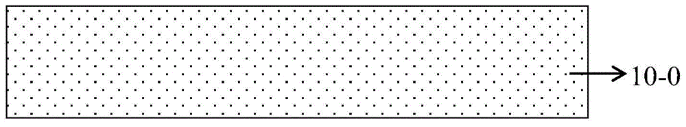
[0063] In the first step, spin-coat the first photoresist layer:

[0064] Spin-coating a photoresist layer on the surface of the planar sapphire LED substrate to form a first photoresist layer covering the surface of the sapphire LED substrate;

[0065] The second step is to make the first photoresist layer with micro-nano dot array:

[0066] Using nanoimprint photolithography technology, the first photoresist layer covering the surface of the sapphire LED substrate obtained in the first step is photolithographically made into a first photoresist layer with an array of micro-nano dots;

[0067] The third step, the first dry etching:

[0068] Using the first photoresist layer with micro-nano dot array obtained in the second step as a mask, use the first dry etching to etch the sapphire LED substrate without the covera...

Embodiment 2

[0081] The method for manufacturing an LED patterned substrate with a double-layer micro-nano array structure in this embodiment, the steps are:

[0082] In the first step, spin-coat the first photoresist layer:

[0083] Spin-coating a photoresist layer on the surface of the planar silicon carbide LED substrate to form a first photoresist layer covering the surface of the silicon carbide LED substrate;

[0084] The second step is to make the first photoresist layer with micro-nano dot array:

[0085] Using the photolithography technology of laser holographic interference exposure, the first photoresist layer covering the surface of the silicon carbide LED substrate obtained in the first step is photolithographically made into a first photoresist layer with an array of micro-nano dots;

[0086] The third step, the first dry etching:

[0087] Using the first photoresist layer with micro-nano dot array obtained in the second step as a mask, use the first dry etching to etch the...

Embodiment 3

[0100] A method for manufacturing an LED patterned substrate with a double-layer micro-nano array structure, the steps are:

[0101] In the first step, spin-coat the first photoresist layer:

[0102] Spin-coating a photoresist layer on the surface of the planar gallium nitride LED substrate to form a first photoresist layer covering the surface of the gallium nitride LED substrate;

[0103] The second step is to make the first photoresist layer with micro-nano dot array:

[0104] Using the photolithography technology of nanosphere self-assembly method, the first photoresist layer covering the surface of the gallium nitride LED substrate obtained in the first step is photolithographically made into the first photoresist layer with a micro-nano dot array;

[0105] The third step, the first dry etching:

[0106] Using the first photoresist layer with micro-nano dot arrays obtained in the second step as a mask, the gallium nitride LED substrate without the coverage of the first ...


PUM

PropertyMeasurementUnit
diameteraaaaaaaaaa
heightaaaaaaaaaa
diameteraaaaaaaaaa

Abstract

The invention discloses a manufacturing method for an LED patterned substrate with a double-layer micro-nano array structure, and relates to a semiconductor device. The manufacturing method comprises the following steps: performing spin-coating to obtain a first photoresist layer; manufacturing a first photoresist layer with a micro-nano spot array; performing primary dry etching; removing the first photoresist layer with the micro-nano spot array by using a wet method; performing spin-coating to obtain a second photoresist layer; manufacturing a second photoresist layer with a micro-nano spot array; performing secondary dry etching; and removing the second photoresist layer with the micro-nano spot array by using the wet method, thus manufacturing the LED patterned substrate with the double-layer micro-nano array structure. According to the method disclosed by the invention, due to the design of the first layer of micro-nano structure, the crystal lattice quality of GaN is improved; due to the design of the second layer of micro-nano structure, the light extraction efficiency of an LED is improved; the defect that the improvement on the crystal lattice quality of GaN and the maximum improvement on the light extraction efficiency of the LED can not be compatible in the prior art is overcome.

Description

technical field [0001] The technical solution of the invention relates to a semiconductor device, in particular to a method for manufacturing an LED patterned substrate with a double-layer micro-nano array structure. Background technique [0002] Light-emitting diodes (hereinafter referred to as LEDs) have been widely valued for their advantages of energy saving and environmental protection. In particular, high-power white light diodes, as the third-generation lighting source, have gradually entered family indoor lighting from outdoor decoration and engineering lighting, and are replacing incandescent and fluorescent lamps. [0003] Although the level of GaN-based LED chips has been greatly developed, there are two key problems: poor gallium nitride crystal quality and low light extraction efficiency, which have hindered its development from beginning to end. The poor lattice quality is due to the fact that GaN has to be grown on heterogeneous substrates such as sapphire, s...

Claims


Application Information

Patent Timeline
Patent Type & Authority Applications(China)
IPC IPC(8): H01L33/02H01L33/22H01L33/00
CPCH01L33/005H01L33/02H01L33/22
Inventor 张勇辉毕文刚张紫辉徐庶耿翀
Owner HEBEI UNIV OF TECH
Why Eureka
Try Eureka