High coupling efficiency electric injection integration silicon-based laser

A high-coupling and laser technology, applied in the structure of optical waveguide semiconductors, the structure of active regions, etc., can solve the problems of large optical coupling loss and small alignment tolerance, and achieve high-efficiency output, compact structure, and simple process. Effect

Active Publication Date: 2016-02-03
WUHAN POST & TELECOMM RES INST CO LTD
View PDF5 Cites 12 Cited by
  • Summary
  • Abstract
  • Description
  • Claims
  • Application Information

AI Technical Summary

Problems solved by technology

[0006] The technical problem to be solved by the present invention is that the optical coupling loss of the current silicon-based flip-chip welding laser is large, and the alignment tolerance between the active chip and the silicon-based chip is small

Method used


Image

  • High coupling efficiency electric injection integration silicon-based laser
  • High coupling efficiency electric injection integration silicon-based laser
  • High coupling efficiency electric injection integration silicon-based laser

Examples


Embodiment 1

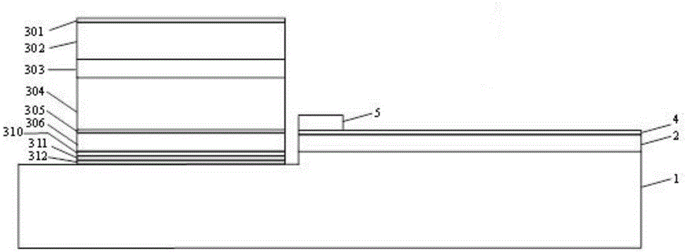
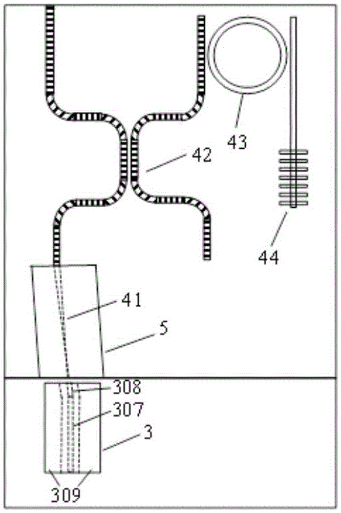
[0047] The low refractive index layer 5 covered on the speckle converter 41 is SiO 2 , both width and thickness are 6 μm. Semiconductor active chips have the following two setups:

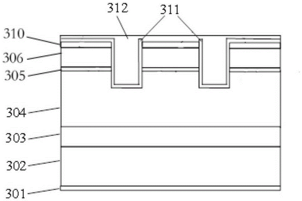
[0048] One is a typical commercial semiconductor active chip. The total thickness of the waveguide on both sides of the active layer is 0.6 μm, the width of the ridge is 5.5 μm, and the output near-field distribution is as follows: Figure 4 shown. The near field is in the direction of the fast axis and the slow axis 1 / e 2 The widths are 1.01μm and 5.09μm respectively, which are elliptical spots;

[0049] The other is a large-mode semiconductor active chip, the thickness of the output waveguide 308 near the active layer is 5 μm, the width of the ridge portion 307 is 5.5 μm, and the output near-field distribution is as follows: Figure 5 shown. The near field is Gaussian-like distribution in both the fast axis and the slow axis direction, and its 1 / e 2 The widths are 4.07 μm and 4.88 μm, respe...


PUM


Abstract

The invention discloses a high coupling efficiency electric injection integration silicon-based laser, which is a laminated structure, and comprises a silicon substrate, an insulating layer, a large speckle semiconductor active chip, top layer silicon and a low refractive index layer. The upper surface of the silicon substrate is provided with a routine part and an etched part which is etched; the insulating layer is arranged on the routine part of the silicon substrate; the large speckle semiconductor active chip is arranged on the etched part of the silicon substrate; the top layer silicon is arranged on the upper surface of the insulating layer; the low refractive index layer is arranged on the side of the upper surface of the top layer silicon proximate to the large speckle semiconductor active chip. The high coupling efficiency electric injection integration silicon-based laser can directly and efficiently output single mode laser, and be commercialized, has the advantages of compact structure, simple process, and high efficiency and stability, and possesses a broad application prospect in the fields such as optical interconnection, optical communication, spectrum determination, optical remote sensing, etc.

Description

technical field [0001] The invention relates to the technical field of semiconductor optoelectronic devices, in particular to an electrical injection integrated silicon-based laser with high coupling efficiency. Background technique [0002] With the rapid increase of global data communication traffic, people have put forward higher requirements for the computing speed of computer systems, which includes the improvement of computing speed, information transmission speed and integration of micro-processing chips. However, as the chip size decreases, the speed of information transmission between chips is limited by the RC (resistance-capacitance, resistance-capacitance) effect of electronic devices, and the overall power consumption of the system gradually increases. Therefore, the traditional electrical interconnection method has gradually become the bottleneck of the overall performance improvement of the high-speed computer system. The proposal and development of optical i...

Claims


Application Information

Patent Timeline
Patent Type & Authority Applications(China)
IPC IPC(8): H01S5/22H01S5/34
Inventor 刘磊肖希王磊邱英李淼峰陈代高杨奇余少华
Owner WUHAN POST & TELECOMM RES INST CO LTD
Why Eureka
Try Eureka