Method of forming mems devices

A device, wet etching technology, used in semiconductor/solid-state device parts, piezoelectric/electrostrictive/magnetostrictive devices, optical components, etc., can solve problems such as poor performance of MEMS devices, and improve the interface characteristics, to ensure accurate timing, to enhance the effect of adhesion

Active Publication Date: 2017-07-14
SEMICON MFG INT (SHANGHAI) CORP
View PDF8 Cites 0 Cited by
  • Summary
  • Abstract
  • Description
  • Claims
  • Application Information

AI Technical Summary

Problems solved by technology

[0006] The problem solved by the present invention is that the performance of MEMS devices in the prior art is not good

Method used


Image

  • Method of forming mems devices
  • Method of forming mems devices
  • Method of forming mems devices

Examples


no. 1 example

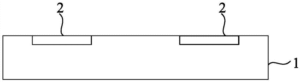
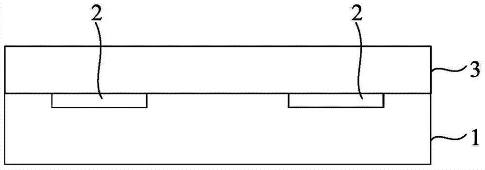
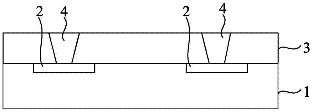
[0065] refer to figure 1 A substrate 1 is provided, and a CMOS device 2 is formed in the substrate 1. The CMOS device 2 is electrically connected to the MEMS device, and is used for outputting signals to the MEMS device and receiving signals output by the MEMS device. The MEMS device to be formed in this embodiment is a resonator or an oscillator, and the resonator will be used as an example for description below.

[0066] It should be noted, figure 1 Among them, the structure indicated by the label 2 is only used to characterize the position of the CMOS device, and cannot be used to describe the shape of the CMOS device.

[0067] In a specific embodiment, the substrate 1 may be a silicon substrate, or may be a germanium, silicon germanium, gallium arsenide or silicon-on-insulator substrate. Those skilled in the art can select the substrate according to needs, so the type of the substrate should not limit the protection scope of the present invention. The substrate 1 in t...

no. 2 example

[0088] The differences between this embodiment and the first embodiment are:

[0089] refer to Figure 11 After forming the SiGe layer 8 and the silicon oxide layer 9 on the SiGe layer 8 on the diffusion barrier layer 6 and in the first through hole, repeat the steps of forming the SiGe layer and thermal oxidation growth to form the silicon oxide layer at least once, so that A multi-layer SiGe layer 8 and a silicon oxide layer 9 are formed on the diffusion barrier layer 6 , wherein the SiGe layer 8 and the silicon oxide layer 9 are distributed vertically at intervals.

[0090] In specific embodiments, each thermal oxidation can be dry oxidation or wet oxidation. The gas used in the dry oxidation process is O 2 , O 3 one or both of them. The relevant parameters in the dry oxidation process are: the gas flow range is 100sccm-250sccm, the temperature range is 400°C-800°C, and the time range is 1min-3min. In this embodiment, the gas flow rate is less than the gas flow rate in...


PUM

PropertyMeasurementUnit
thicknessaaaaaaaaaa
thicknessaaaaaaaaaa
frequency temperature coefficientaaaaaaaaaa

Abstract

The invention discloses a forming method of an MEMS (Micro-Electro-Mechanical System) device. The method comprises the following steps: providing a substrate, wherein CMOS (Complementary Metal Oxide Semiconductor) devices are formed in the substrate; forming a sacrificial layer on the substrate; forming first through holes in the sacrificial layer, wherein the first through holes are positioned in the CMOS devices; forming a SiGe layer on the sacrificial layer and in the first through holes, wherein the first through holes are fully filled with the SiGe layer; generating a silicon oxide layer on the SiGe layer through a thermal oxide growth process; and after the silicon oxide layer is formed, removing the sacrificial layer. SiO<2> generated by the thermal oxide growth process is combined with SiGe by bonding, so that an interface characteristic between the silicon oxide layer and the SiGe layer can be enhanced, the bonding force between the silicon oxide layer and the SiGe layer is enhanced, and the problem of peeling is solved in comparison to SiO<2> formed by chemical vapor deposition.

Description

technical field [0001] The invention relates to the technical field of semiconductors, in particular to a method for forming a MEMS device. Background technique [0002] Radio frequency microelectromechanical system (RF MEMS) is an RF product processed by MEMS technology, and it is one of the important application fields of MEMS technology. In existing RF MEMS, such as resonators and oscillators, radio frequency frequencies can be generated to generate clock outputs for timing purposes. [0003] Taking resonators as an example, usually resonators include quartz crystal resonators and ceramic resonators, wherein quartz crystal resonators can provide smaller device sizes to increase integration and reduce production costs. However, quartz crystal resonators are not conducive to integration into integrated circuits, so the prior art proposes to use SiGe to manufacture resonators, which is beneficial to the integration of resonators into integrated circuits. [0004] However, ...

Claims


Application Information

Patent Timeline
Patent Type & Authority Patents(China)
IPC IPC(8): B81C1/00B81B7/02
Inventor 何昭文李曼曼
Owner SEMICON MFG INT (SHANGHAI) CORP
Why Eureka
Try Eureka