Planar VDMOS device and manufacturing method thereof
A planar, device technology, applied in semiconductor/solid-state device manufacturing, semiconductor devices, electrical components, etc., can solve problems affecting the dynamic characteristics of power devices, affecting VDMOS parameters, etc., to reduce parasitic capacitance, reduce effective area, reduce The effect of small conduction losses
- Summary
- Abstract
- Description
- Claims
- Application Information
AI Technical Summary
Problems solved by technology
Method used
Image

Examples
Embodiment 1
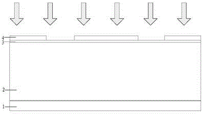
[0054] image 3 The process flow of a method for manufacturing a planar VDMOS device disclosed in the present invention specifically includes the following steps:
[0055] Step 101, forming a gate oxide layer on the epitaxial layer, and forming a polysilicon layer on the gate oxide layer;
[0056] Step 102, etching the polysilicon layer to form a polysilicon gate;
[0057] Step 103, performing ion implantation to form a doped polysilicon gate;
[0058] Step 104, forming a photoresist mask on the surface of the doped polysilicon gate;
[0059] Step 105, etching a polysilicon gate trench on the doped polysilicon gate;
[0060] Step 106 , performing thermal oxidation on the polysilicon gate trench and the surface of the doped polysilicon gate to form an oxide layer.
[0061] Preferably, a layer of photoresist is coated on the doped polysilicon gate and the gate oxide layer, and then the photoresist is exposed through a mask plate to form a photoresist mask, and dry etching is...
Embodiment 2
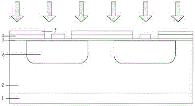
[0067] This embodiment provides a method for manufacturing a planar VDMOS device, and its specific process is as follows Figure 4 Shown:
[0068] In step 201, an epitaxial layer of the first conductivity type is formed on the upper surface of the substrate of the first conductivity type.
[0069] In this embodiment, a substrate of the first conductivity type can be provided first, and an epitaxial layer of the first conductivity type is formed on the substrate of the first conductivity type. The substrate of the first conductivity type can be an N-type substrate or a P-type substrate. substrate, when the substrate of the first conductivity type is an N-type substrate, the first conductive epitaxial layer disposed on the N-type substrate is an N-type epitaxial layer; when the substrate of the first conductivity type is a P-type When the substrate is used, the first conductive epitaxial layer disposed on the P-type substrate is a P-type epitaxial layer.
[0070] In step 202, ...
Embodiment 3
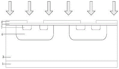
[0101] The present invention also provides a planar VDOMS device, at least comprising the following structures:
[0102] A gate structure consisting of a gate oxide layer and a doped polysilicon gate;
[0103] The oxide layer in the gate structure divides the doped polysilicon gate into multiple parts;
[0104] The bottom of the polysilicon gate trench is in contact with the surface of the gate oxide layer.
PUM
| Property | Measurement | Unit |
|---|---|---|
| Groove depth | aaaaa | aaaaa |
| Depth | aaaaa | aaaaa |
| Thickness | aaaaa | aaaaa |
Abstract
Description
Claims
Application Information
 - R&D
- Intellectual Property
- Life Sciences
- Materials
- Tech Scout
- Unparalleled Data Quality
- Higher Quality Content
- 60% Fewer Hallucinations
Browse by: Latest US Patents, China's latest patents, Technical Efficacy Thesaurus, Application Domain, Technology Topic, Popular Technical Reports.
© 2025 PatSnap. All rights reserved.Legal|Privacy policy|Modern Slavery Act Transparency Statement|Sitemap|About US| Contact US: help@patsnap.com