
TFT substrate manufacturing method and TFT substrate

A manufacturing method and substrate technology, which are applied in semiconductor/solid-state device manufacturing, electrical components, electric solid-state devices, etc., can solve the problems of low poly-Si gap state density, poor TFT characteristics, easy deformation of the substrate, etc., and achieve improved Crystallization effect, shortened crystallization time, good ohmic contact effect

Active Publication Date: 2016-02-24
SHENZHEN CHINA STAR OPTOELECTRONICS TECH CO LTD
View PDF4 Cites 6 Cited by
  • Summary
  • Abstract
  • Description
  • Claims
  • Application Information

AI Technical Summary

Problems solved by technology

[0006] At present, the commonly used crystallization processes of amorphous silicon (a-Si) include chemical vapor deposition (CVD), excimer laser crystallization (ELA), solid phase crystallization (SPC), metal induced crystallization (MIC), and metal lateral induction. However, the poly-Si crystal grain size produced by CVD crystallization process is extremely small, and the deposition rate is low; the traditional SPC crystallization process requires high temperature and takes a long time, resulting in easy deformation of the substrate and high cost; The poly-Si layer produced by the MIC and MILC crystallization processes has large metal residues, resulting in poor TFT characteristics; the poly-Si produced by the ELA crystallization process has a low gap state density, expensive equipment, and it is difficult to produce large-area poly-Si films.

Method used


Image

  • TFT substrate manufacturing method and TFT substrate
  • TFT substrate manufacturing method and TFT substrate
  • TFT substrate manufacturing method and TFT substrate

Examples


Embodiment Construction

[0042] In order to further illustrate the technical means adopted by the present invention and its effects, the following describes in detail in conjunction with preferred embodiments of the present invention and accompanying drawings.

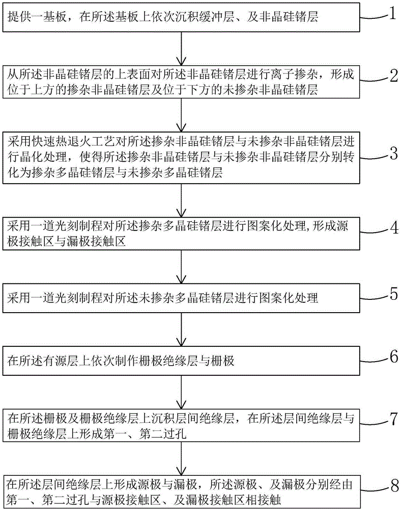
[0043] see figure 2 , the invention provides a kind of manufacturing method of TFT substrate, comprises the following steps:

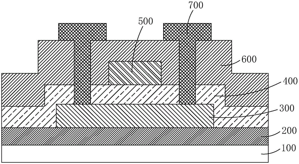
[0044] Step 1, such as image 3 As shown, a substrate 10 is provided, and a buffer layer 20 and an amorphous silicon germanium (a-SiGe) layer 30 are sequentially deposited on the substrate 10 .

[0045] Preferably, the substrate 10 is a glass substrate.

[0046] Preferably, the buffer layer 20 is silicon oxide (SiO x ) layer, silicon nitride (SiN x ) layer, or a composite layer composed of a silicon oxide layer and a silicon nitride layer.

[0047] Step 2, such as Figure 4 As shown, the amorphous silicon germanium layer 30 is ion-doped from the upper surface of the amorphous silicon germanium layer 30, thereby ...


PUM


Abstract

The invention provides a TFT substrate manufacturing method and a TFT substrate. The TFT substrate manufacturing method comprises the steps of depositing a buffer layer and an amorphous silicon germanium layer on a substrate; implanting doped ions at the upper portion of the amorphous silicon germanium layer so as to form a doped amorphous silicon germanium layer; employing a rapid thermal annealing process for crystallization processing on the doped amorphous silicon germanium layer and the un-doped amorphous silicon germanium layer. Because the crystallization process begins from the doped amorphous silicon germanium layer and the crystallization temperature of the doped amorphous silicon germanium layer is low, the crystallization process can be carried out at a low temperature; because the un-doped amorphous silicon germanium layer in contact with the doped amorphous silicon germanium layer can be crystallized continuously at the low temperature, the doped polysilicon germanium layer and the un-doped polysilicon germanium layer can be obtained; compared with prior art, like existing solid phase crystallization, the crystallization process of the present invention can be carried out at a lower temperature, and the crystallization time can be shortened; the crystallization effect can be improved; and larger and more uniform crystal grains can be obtained.

Description

technical field [0001] The invention relates to the field of display technology, in particular to a manufacturing method of a TFT substrate and the TFT substrate. Background technique [0002] With the development of display technology, liquid crystal displays (Liquid Crystal Display, LCD) and other flat display devices are widely used in mobile phones, TVs, personal digital assistants due to their advantages of high image quality, power saving, thin body and wide application range. , digital cameras, notebook computers, desktop computers and other consumer electronics products have become the mainstream of display devices. [0003] Most of the liquid crystal display devices currently on the market are backlight liquid crystal displays, which include a liquid crystal display panel and a backlight module. The working principle of the liquid crystal display panel is to place liquid crystal molecules between two parallel glass substrates. There are many vertical and horizontal...

Claims


Application Information

Patent Timeline
Patent Type & Authority Applications(China)
IPC IPC(8): H01L21/77H01L27/12
CPCH01L27/1229H01L27/1274H01L27/1285
Inventor 李亚徐源竣
Owner SHENZHEN CHINA STAR OPTOELECTRONICS TECH CO LTD
Learn More