Plasmon enhancement based electron emitting device and method with light enhancement/modulation

A technology of plasmon enhancement and optical modulation device, which is applied to the structure of electron emission electrode/cathode and optical resonant cavity, can solve the problems of inability to achieve ultrafast electron source and low quantum efficiency of noble metal cathode, and achieve the improvement of electron emission. The effect of emission efficiency

Active Publication Date: 2016-03-09
SOUTHEAST UNIV
View PDF4 Cites 8 Cited by
  • Summary
  • Abstract
  • Description
  • Claims
  • Application Information

AI Technical Summary

Problems solved by technology

In order to obtain an electron source with modulation characteristics, the external voltage can be modulated by electrical methods to achieve modulation characteristics, but this method cannot meet the requirements of ultrafast electron sources due to the limitation of the frequency characteristics of the electrical device itself; in addition to electrical modulation, it can also be used The photon characteristics of the incide

Method used


Image

  • Plasmon enhancement based electron emitting device and method with light enhancement/modulation
  • Plasmon enhancement based electron emitting device and method with light enhancement/modulation

Examples


Embodiment 1

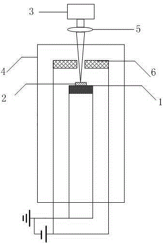
[0025] Example 1: A layer of carbon nanotubes is prepared by screen printing on the surface of the oxygen-free copper substrate, and then a composite cathode structure is formed after the golden triangular plate particle solution is deposited on the surface of the carbon nanotubes by a drop-coating method. according to figure 1 For packaging, the laser irradiates the surface of the composite cathode through the collimation system and the anode containing through holes. Due to the local field enhancement characteristics of the silver nanotriangular plate, a local field that is much greater than the incident laser light field will be formed on the surface of the composite cathode. Carbon nano Under the common potential barrier compression of the local field and the applied voltage, the tube will produce enhanced electron emission.

Embodiment 2

[0026] Example 2: A layer of carbon nanotube film is prepared by chemical vapor deposition on the surface of a silicon wafer containing an iron-nickel catalyst, and then gold nanoparticles are prepared on the surface of the carbon nanotube by evaporation and annealing to form a composite cathode structure. The cathode structure according to figure 1 For packaging, the laser irradiates the surface of the composite cathode through the collimation system and the anode containing through holes. Due to the local field enhancement characteristics of gold nanoparticles, a local field that is much greater than the incident laser light field will be formed on the surface of the composite cathode. Under the common potential barrier compression of the local field and the applied voltage, the tube will produce enhanced electron emission.

Embodiment 3

[0027] Embodiment 3: transfer a layer of graphene material on the surface of the ITO conductive glass substrate, then use the method of spin coating to spin coat a layer of gold nano-star solution on the graphene surface, and dry to form a composite cathode structure of graphene and gold nano-star . The cathode structure according to figure 1 For packaging, the laser passes through the collimation system and the anode containing through holes to irradiate the surface of the composite cathode. Due to the local field enhancement characteristics of gold nanostars, a local field that is much greater than the intensity of the incident laser light field will be formed on the surface of the composite cathode. Electron emission will occur under the common potential barrier compression of the local field and the applied voltage. By changing the intensity of the incident laser, changing the local electric field of the metal nanostructure and the electric field around the graphene, the ...


PUM


Abstract

The present invention discloses a plasmon enhancement based electron emitting device and method with light enhancement/modulation. The device includes: a package structure, a power source and a light source, wherein the package structure has a cathode and an anode; a through hole is formed in the anode, the cathode is disposed on a conductive substrate, and the cathode is a field-emission cathode constituted by a cathode substrate and metal nanostructures attached to a surface of the cathode substrate; the power source forms an electric field between the cathode and the anode; and the light source emits laser light incident on the metal nanostructures of the cathode through the through hole of the anode. In the light enhancement/modulation electron emission device of the present invention, the incident light emitted by the light source causes enhancement of the electron emission of the field-emission cathode which is formed by combination of field-emission material of the cathode substrate and the metal nanostructures, so that the electron emission efficiency is increased. Meanwhile, by changing the intensity, wavelength and polarization of the incident laser, a local field of the surface of the field-emission material is adjusted, and light modulating electron emission is achieved.

Description

technical field [0001] The light enhancing / modulating electron emission device of the present invention can be applied to high-frequency electronic devices, ultrafast electron sources, and free electron lasers. Background technique [0002] For the field electron emission of fixed materials, the emission ability is mainly determined by the potential barrier between the cathode material and the vacuum level, the energy of the internal electrons and the magnitude of the external electric field. The higher the energy of the internal free electrons, the greater the external electric field. Larger, the easier it is for electrons to tunnel to the vacuum level. In order to obtain an electron source with modulation characteristics, the external voltage can be modulated by electrical methods to achieve modulation characteristics, but this method cannot meet the requirements of ultrafast electron sources due to the limitation of the frequency characteristics of the electrical device i...

Claims


Application Information

Patent Timeline
IPC IPC(8): H01S5/10H01J19/02
CPCH01J19/02H01S5/10
Inventor 王琦龙翟雨生杜小飞齐志央李晓华
Owner SOUTHEAST UNIV
Why Eureka
Try Eureka