

Light-emitting diode and its preparation method
A technology for light-emitting diodes and a manufacturing method, which is applied in the fields of semiconductor/solid-state device manufacturing, organic semiconductor devices, electric solid-state devices, etc., can solve the problem that the electrical properties of light-emitting diode elements cannot meet application requirements, and the multi-color output combination of the same chip cannot be realized. The growth temperature of the type layer cannot be reached, so as to achieve the effect of improving the light extraction efficiency, lowering the growth temperature, and reducing the lattice difference.
- Summary
- Abstract
- Description
- Claims
- Application Information
AI Technical Summary
Problems solved by technology
Method used
Image

Examples
Embodiment 1
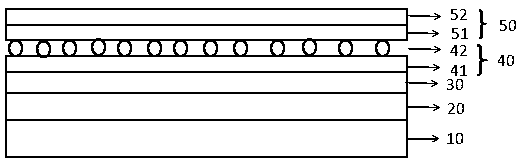
[0032] See attached figure 1 , the light emitting diode structure includes a substrate 10, the substrate 10 is sapphire, silicon carbide, silicon, gallium nitride and other materials; an N-type semiconductor layer 20 is placed on the upper surface of the substrate 10, and the N-type semiconductor layer 20 is a single layer structure or a multilayer structure with different doping concentrations; the stress release layer 30 is placed on the upper surface of the N-type semiconductor layer 20, and the stress release layer 30 is an InGaX / GaX cycle structure; the transition layer 41 with a thickness of 10-100 Å The upper surface of the release layer 30 is grown, and the material of the transition layer 41 is Al x In y GaX, wherein 0≤x<1, 0<y<1, said X is a group V element. The nanoparticle layer 42 is placed on the upper surface of the transition layer 41, and forms the luminescent layer 40 with the transition layer 41. The nanoparticle layer 42 is one or more of spherical partic...
Embodiment 2
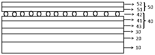
[0043] The difference between this embodiment and Embodiment 1 is that in this embodiment, after the growth of the stress release layer 30 is completed, the InGaX / GaX multi-quantum well layer 43 is first deposited by MOCVD, and then a transition layer is grown on the surface of the multi-quantum well layer 43. layer 41, the material of the transition layer 41 is Al x In y GaX material, wherein 0≤x<1, 0<y<1, and then using physical deposition to deposit the nanoparticle layer 42; the multi-quantum well layer 43, the transition layer 41 and the nanoparticle layer 42 together form the light-emitting layer 40; finally A P-type layer 50 composed of a hole injection layer 51 and a hole transport layer 52 is deposited to form a light emitting diode structure.
[0044] In the present embodiment, the In composition in the InGaX / GaX multi-quantum well layer 43, the In composition in the transition layer 41, and the particle diameter of the nanoparticle layer 42 are adjusted so that the...
PUM
 Abstract
Description
Claims
Application Information