

Method for preparing black silicon material
A technology of black silicon and silicon film, which is applied in the field of black silicon material preparation, can solve problems such as affecting the doping content of black silicon, and achieve the effects of increasing the doping content, increasing the absorption rate and reducing volatilization
- Summary
- Abstract
- Description
- Claims
- Application Information
AI Technical Summary
Problems solved by technology
Method used
Image

Examples
Embodiment Construction
[0024] The present invention will be described in detail below in conjunction with the accompanying drawings.
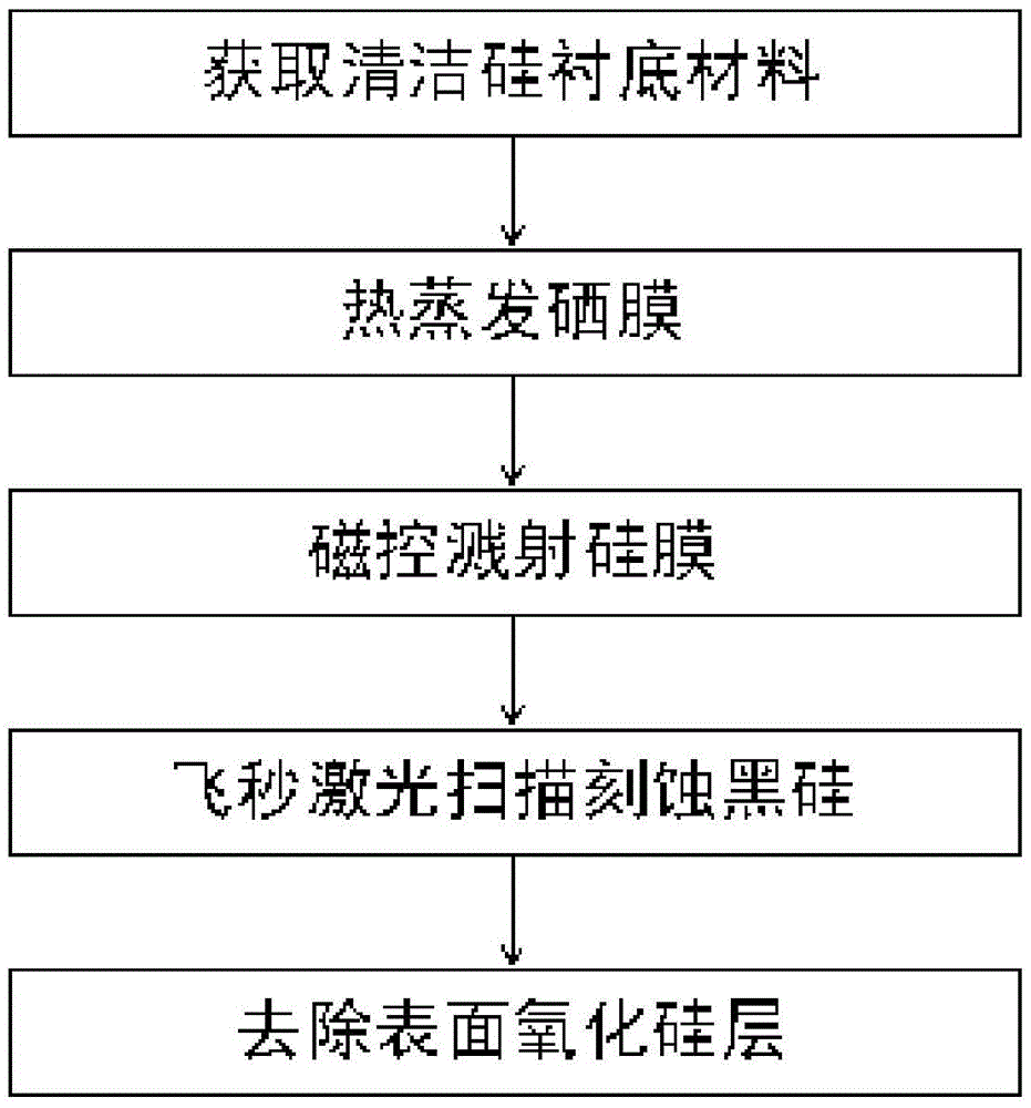
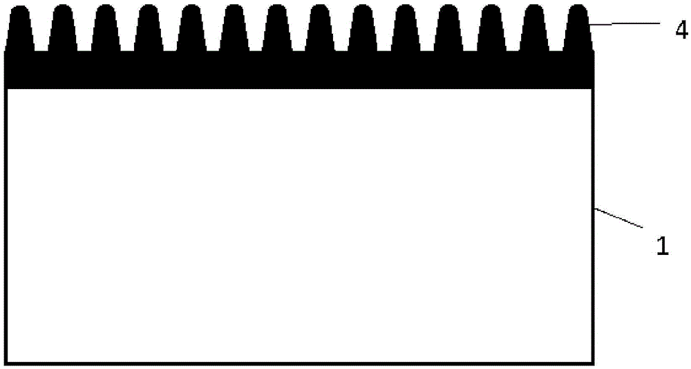
[0025] Such as figure 1 Shown is a schematic flow chart of this embodiment.
[0026] Step 1: Obtain a clean silicon substrate.
[0027] N-type silicon chip doped with phosphorus is selected as the substrate material. Then use the RCA standard cleaning method to clean the silicon substrate to remove the surface oxide. Then put the cleaned silicon substrate into acetone for 10 minutes to sonicate to remove the residual organic matter on the surface. Finally, the silicon substrate was sonicated in deionized water for 5 minutes and dried under nitrogen atmosphere.
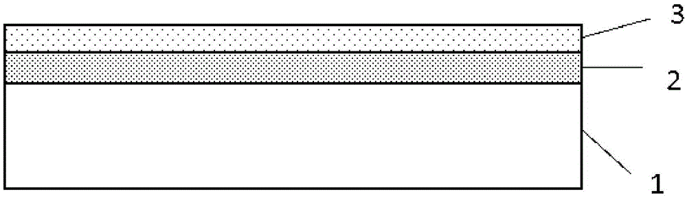
[0028] Step 2: Thermally evaporated selenium film
[0029] Put the silicon substrate cleaned in step 1 on the workbench of the vacuum evaporation device, and evacuate the vacuum of the vacuum chamber to 6×10 -4 Pa. Start the evaporation unit, and evaporate a layer of 100nm selenium film on the polished...
PUM
| Property | Measurement | Unit |
|---|---|---|
| thickness | aaaaa | aaaaa |
| thickness | aaaaa | aaaaa |
Abstract
Description
Claims
Application Information