Dual perovskite/copper-indium-gallium-selenium solar battery
A solar cell, copper indium gallium selenide technology, applied in the field of solar cells, can solve the problems of toxicity, unsuitability for mass production, "selenium loss" and other problems
- Summary
- Abstract
- Description
- Claims
- Application Information
AI Technical Summary
Problems solved by technology
Method used
Image
Examples
Embodiment Construction
[0019] The technical solution will be described in detail below in conjunction with the accompanying drawings and embodiments.
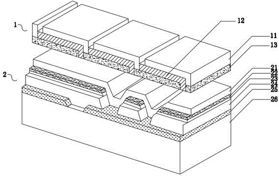
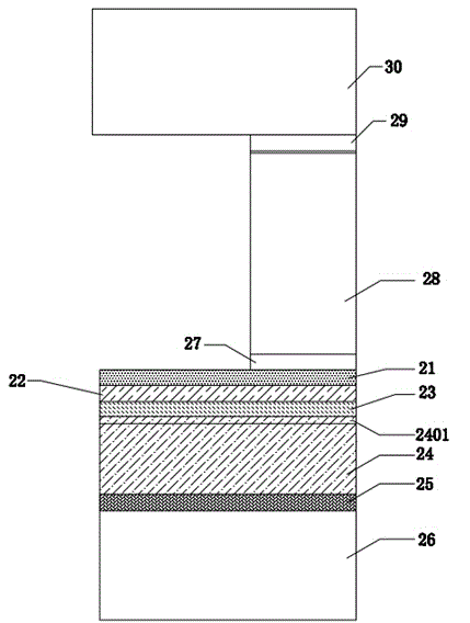
[0020] Please refer to the attached figure 1 , a dual-junction perovskite and copper indium gallium selenide solar cell of the present invention, which comprises: an upper perovskite layer 1, a lower copper indium gallium selenide layer 2, the perovskite layer 1 and copper indium gallium selenide In layer 2, the two node layers are overlapped, and a transparent insulating layer is arranged in the middle. The perovskite layer 1 includes an upper transparent conductive layer 11, a perovskite absorbing layer 12, and a lower transparent conductive layer 13 that are sequentially laminated together; the copper indium gallium selenide layer 2 includes zinc oxide doped layers that are sequentially laminated together. Aluminum conductive layer 21 , zinc oxide layer 22 , cadmium sulfide film layer 23 , copper indium gallium selenium absorption layer 24 , moly...
PUM
| Property | Measurement | Unit |
|---|---|---|
| Thickness | aaaaa | aaaaa |
| Thickness | aaaaa | aaaaa |
| Thickness | aaaaa | aaaaa |
Abstract
Description
Claims
Application Information


