An ultra-thin channel trench tunneling field effect transistor

A tunneling field effect and transistor technology, which is applied in the direction of transistors, semiconductor devices, electrical components, etc., can solve the problems of reducing the short channel effect

Active Publication Date: 2018-10-12
HANGZHOU DIANZI UNIV
View PDF4 Cites 0 Cited by
  • Summary
  • Abstract
  • Description
  • Claims
  • Application Information

AI Technical Summary

Problems solved by technology

When the feature size is reduced to sub-10nm, it is difficult to effectively reduce the short channel effect simply by increasing the gate control capability

Method used


Image

  • An ultra-thin channel trench tunneling field effect transistor
  • An ultra-thin channel trench tunneling field effect transistor
  • An ultra-thin channel trench tunneling field effect transistor

Examples


Embodiment Construction

[0016] In order to make the purpose, technical solution and advantages of the present invention clearer, the present invention will be described in detail below in conjunction with the accompanying drawings.

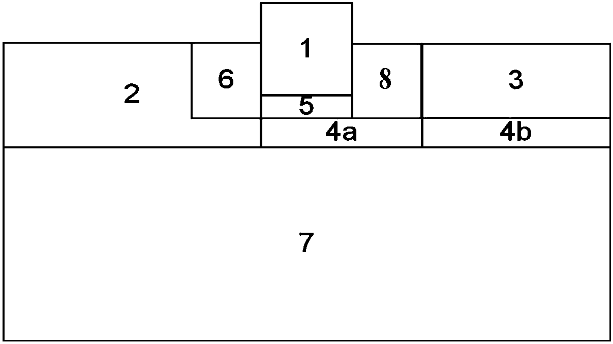
[0017] Such as figure 1 As shown, an ultra-thin channel groove tunneling field effect transistor is characterized in that it includes a gate 1, a source region 2, a drain region 3, a first channel region 4a, a second channel region 4b, and a gate dielectric layer 5. The first isolation layer 6 and the buried oxide layer 7; the gate dielectric layer 5 is provided under the gate 1, the gate 1 and the gate dielectric layer 5 are located on the first channel region 4a, and the first isolation layer 6 will The gate 1 is isolated from the source region 2, and the second isolation layer 8 isolates the gate 1 from the drain region 3; the thickness of the first isolation layer 6 and the second isolation layer 8 is not less than the thickness of the gate dielectric layer 5; the se...


PUM


Abstract

The invention discloses an ultrathin channel groove tunneling field effect transistor which is composed of a grid electrode, a source region, a drain region, a first channel region, a second channel region, a grid dielectric layer, a first isolating layer, a second isolating layer and buried oxide layer, wherein the grid electrode and the grid dielectric layer arranged on the position of the channel regions, and the isolation layers are arranged at the two sides of the grid electrode. The new structure has an ultrathin channel so that coupling of the grid electrode and the channel can be enhanced, and thus control capability of the grid electrode can be enhanced and tunneling current of a device can be increased. Another characteristic of the structure is that the intrinsic region (low-doped region) of the channel extends to the drain region. In a word, compared with conventional tunneling transistors, the device of the structure is obviously improved in the aspects of the electrical characteristics of subthreshold swing and switching current ratio and stability.

Description

technical field [0001] The invention relates to a device for semiconductor integrated circuits, mainly an ultra-thin channel groove field effect transistor. Background technique [0002] With the development of integrated circuits, the degree of circuit integration is required to be continuously improved, which in turn requires the feature size of semiconductor devices to be continuously reduced. However, devices will face some serious problems in small sizes, such as MOSFET, which is one of the most basic devices constituting integrated circuits, will have short channel effects, leakage-induced barrier lowering effects and other adverse effects in smaller feature sizes. Phenomena, these effects will increase the power consumption of the device and even make the device unable to switch effectively or fail. At present, a common method to reduce power consumption is to reduce the operating voltage while ensuring the driving current, which means reducing the threshold voltage ...

Claims


Application Information

Patent Timeline
Patent Type & Authority Patents(China)
IPC IPC(8): H01L29/772H01L29/06H01L29/10
CPCH01L29/06H01L29/0607H01L29/10H01L29/1029H01L29/772
Inventor 王颖曹菲王艳福于成浩
Owner HANGZHOU DIANZI UNIV
Why Eureka
Try Eureka