Method for real-time patterning of nitride growth silicon substrate

A patterning and nitride technology, applied in gaseous chemical plating, coating, electrical components, etc., can solve the problems of unsuitability for commercial application of silicon-based nitride semiconductor devices, increase manufacturing costs, and complex process, and reduce The effect of threading dislocation density, improving crystal quality, and reducing defect density

Active Publication Date: 2016-07-13
SHANGHAI SIMGUI TECH
View PDF10 Cites 3 Cited by
  • Summary
  • Abstract
  • Description
  • Claims
  • Application Information

AI Technical Summary

Problems solved by technology

The above-mentioned process is complicated, which greatly increases the manufacturing cost, and the pattern is limited by the photolithography layout, which is extremely unsuitable for the commercial application of silicon nitride semiconductor devices

Method used


Image

  • Method for real-time patterning of nitride growth silicon substrate
  • Method for real-time patterning of nitride growth silicon substrate
  • Method for real-time patterning of nitride growth silicon substrate

Examples


Embodiment Construction

[0021] The specific implementation of the method for real-time patterning of a silicon nitride growth substrate provided by the present invention will be described in detail below with reference to the accompanying drawings.

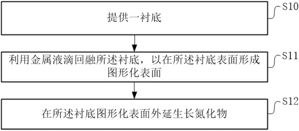
[0022] see figure 1 The method for real-time patterning of a silicon nitride growth substrate in the present invention includes the following steps: step S10, providing a substrate; step S11, using metal droplets to melt back the substrate to form a substrate on the surface of the substrate. Patterned surface; step S12 , epitaxially growing nitride on the patterned surface of the substrate.

[0023] Figure 2A ~ Figure 2D It is a process flow chart of the method for real-time patterning of a nitride growth silicon substrate according to the present invention.

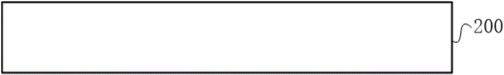
[0024] See step S10 and Figure 2A , providing a substrate 200 . The substrate 200 may be sapphire, silicon carbide, silicon, lithium aluminate, or gallium arsenide.

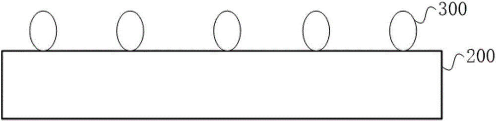
[0025] Refer to step S1...


PUM

PropertyMeasurementUnit
sizeaaaaaaaaaa

Abstract

The invention provides a method for real-time patterning of a nitride growth silicon substrate. The method comprises the following steps that (a) a substrate is provided; (b) back melting of the substrate is performed by utilizing metal liquid drops so that a patterned surface is formed on the surface of the substrate; and (c) epitaxial growth of nitride on the patterned surface of the substrate is performed. The advantages of the method are that a metal organic source is piped in the real-time growth process of the substrate, and the metal atoms are aggregated into the nanoscale liquid drops and uniformly combined on the surface of the substrate in high density. The metal liquid drops and the substrate form alloy under high temperature to corrode the substrate into an uneven surface so that stress caused by crystal lattice mismatch in the heteroepitaxial growth process of the substrate and a nitride epitaxial layer can be alleviated, and the epitaxial layer is enabled to be effectively relaxed. Meanwhile, penetrating dislocation density in the epitaxial layer can also be reduced so that defect density in the nitride epitaxial layer material can be reduced, the crystal quality of the material can be enhanced, and thus the optical and electrical properties of a device can be improved.

Description

technical field [0001] The invention relates to the field of semiconductors, in particular to a method for real-time patterning of a nitride growth silicon substrate. Background technique [0002] Group III-V wide bandgap semiconductor materials represented by gallium nitride (GaN) have developed rapidly in recent years. GaN has the characteristics of wide band gap, direct band gap, good chemical stability and thermal stability. It has important and extensive application potential. [0003] Since GaN and aluminum nitride (AlN) and other intrinsic bulk single crystal materials are difficult to obtain, the current nitride thin film materials are mainly grown on sapphire, silicon carbide, silicon (Si), zinc oxide or gallium arsenide substrates. . Due to the lack of matching substrates for GaN-based epitaxial materials, the crystal quality needs to be further improved. [0004] Silicon materials are the cornerstone of today's microelectronics technology. Silicon material is...

Claims


Application Information

Patent Timeline
Patent Type & Authority Applications(China)
IPC IPC(8): H01L21/205C23C16/44H01L33/22
CPCC23C16/44H01L21/0254H01L21/0262H01L33/22
Inventor 闫发旺张峰赵倍吉谢杰
Owner SHANGHAI SIMGUI TECH
Why Eureka
Try Eureka