Application of electron-beam induced plasma probes to inspection, test, debug and surface modifications

A plasma and electron beam technology, which is used in the field of applying electron beam induced plasma probes for inspection, testing, debugging and surface modification, which can solve the problems of high system cost, large factory occupied area, affecting processing capacity, etc.

Inactive Publication Date: 2016-07-20
ORBOTECH LTD +1
View PDF6 Cites 3 Cited by
  • Summary
  • Abstract
  • Description
  • Claims
  • Application Information

AI Technical Summary

Problems solved by technology

This technique involves large vacuum enclosures and complex electron optics, resulting in high system cost, large factory footprint, and potential impact on throughput

Method used


Image

  • Application of electron-beam induced plasma probes to inspection, test, debug and surface modifications
  • Application of electron-beam induced plasma probes to inspection, test, debug and surface modifications
  • Application of electron-beam induced plasma probes to inspection, test, debug and surface modifications

Examples


Embodiment Construction

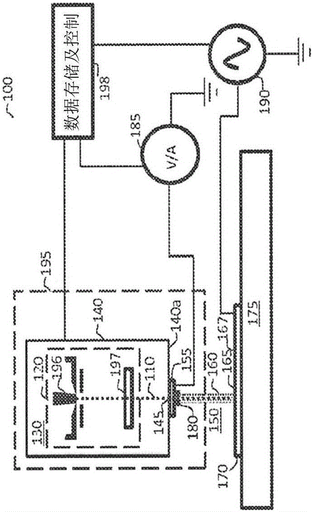
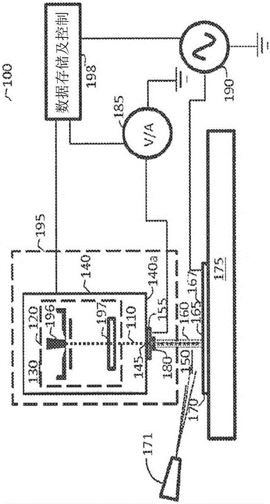
[0038] Various embodiments described below provide solutions based on high-resolution, high-sensitivity, and compact atmospheric electron beam-induced plasma probe technology. This technique essentially relies on the fact that the cool plasma (several eV) generated by an electron beam-driven impact ionization event in air acts as a non-mechanically conductive contact, allowing measurement of the device under test via the resulting secondary plasma electron current ( voltage on the DUT). As the name implies, this technology does not require the DUT to be held in a vacuum. Instead, only the electron emitter (cathode) and electron optics need be kept in the vacuum enclosure. Furthermore, the implementation of this technique requires only a simple electro-optical configuration (eg extraction grid and electrostatic lens) to keep the cost of the gun low and its size (and thus the size of the housing) compact. The electron beam exits the vacuum enclosure containing the electron gun...


PUM


Abstract

An electron-beam induced plasmas is utilized to establish a non-mechanical, electrical contact to a device of interest. This plasma source may be referred to as atmospheric plasma source and may be configured to provide a plasma column of very fine diameter and controllable characteristics. The plasma column traverses the atmospheric space between the plasma source into the atmosphere and the device of interest and acts as an electrical path to the device of interest in such a way that a characteristic electrical signal can be collected from the device. Additionally, by controlling the gases flowing into the plasma column the probe may be used for surface modification, etching and deposition.

Description

technical field [0001] Various embodiments of the invention relate generally to non-mechanical contact detection of electronic devices and surface modification of devices and tissues. In particular, various embodiments relate to the use of electron beam induced plasma probes for metrology and surface modification. Background technique [0002] The ability to measure and apply voltages and currents on patterned structures without having to establish mechanical contact has implications for functional (electrical) testing of semiconductor devices and flat panel displays such as liquid crystal and organic light emitting diode (OLED) displays, backplanes, and printed circuit boards. Significant because non-mechanical contact probing minimizes the possibility of damaging the device / panel under test and also helps to increase test throughput. [0003] Voltage from PhotonDynamics (Orbotech company) Optical systems (VIOS) employ optoelectronic transducers to convert the electric f...

Claims


Application Information

Patent Timeline
Patent Type & Authority Applications(China)
IPC IPC(8): G01R31/308
CPCG01R31/305H01J33/00H01J2237/164H01J2237/188H01J2237/317H01J37/3233H01J37/32825H05H2240/10H05H2245/40G01R1/072G01R31/2825G01N27/70H01J37/32449H01J2237/063
Inventor 内达尔·沙利丹尼尔·托特安利奎·史特林罗南·洛温格斯里蓝·奎许那瓦米艾利·葛雷瑟
Owner ORBOTECH LTD
Why Eureka
Try Eureka