Antimony sulfide/silicon tandem solar cell and preparation method thereof

A technology of stacking solar and antimony sulfide, which is applied in circuits, photovoltaic power generation, electrical components, etc., can solve the problem of no research reports on antimony sulfide/silicon stacked solar cells, and achieve the goal of reducing capital investment, saving resources, and accelerating promotion. Effect

Active Publication Date: 2016-07-27
湖南铱太科技有限公司
View PDF5 Cites 19 Cited by
  • Summary
  • Abstract
  • Description
  • Claims
  • Application Information

AI Technical Summary

Problems solved by technology

However, because it is difficult to find a suitable electrode material that can not only realize the series connection of antimony sulfide thin film solar cells and crystalline silicon solar cells, but also be compatible with the two su

Method used


Image

  • Antimony sulfide/silicon tandem solar cell and preparation method thereof
  • Antimony sulfide/silicon tandem solar cell and preparation method thereof
  • Antimony sulfide/silicon tandem solar cell and preparation method thereof

Examples


Embodiment 1

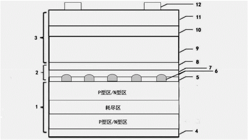
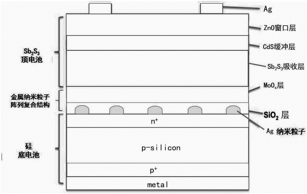
[0049] The upper surface of the crystalline silicon cell that has not undergone texturing, passivation and metallization is routinely cleaned, and an Ag metal layer is prepared on the surface by magnetron sputtering. Using Ag as the target material, DC sputtering is adopted, the sputtering power is 80w, the air pressure is 0.5Pa, the substrate temperature is normal temperature, the distance between the target and the substrate is 10cm, and the sputtering time is 8min to form an Ag metal layer with a thickness of about 100nm.

[0050] Thermal annealing is performed on the Ag metal layer, and annealed at 500° C. for 40 minutes in an argon atmosphere to form a metal nanoparticle array.

[0051] Anneal at 100°C for 10 minutes in an air atmosphere to oxidize the upper surface of the crystalline silicon cell to form SiO 2 layer.

[0052] Metal nanoparticles and SiO by thermal evaporation 2 Preparation of MoO on the surface of the composite layer x layer, using Mo metal as the eva...

Embodiment 2

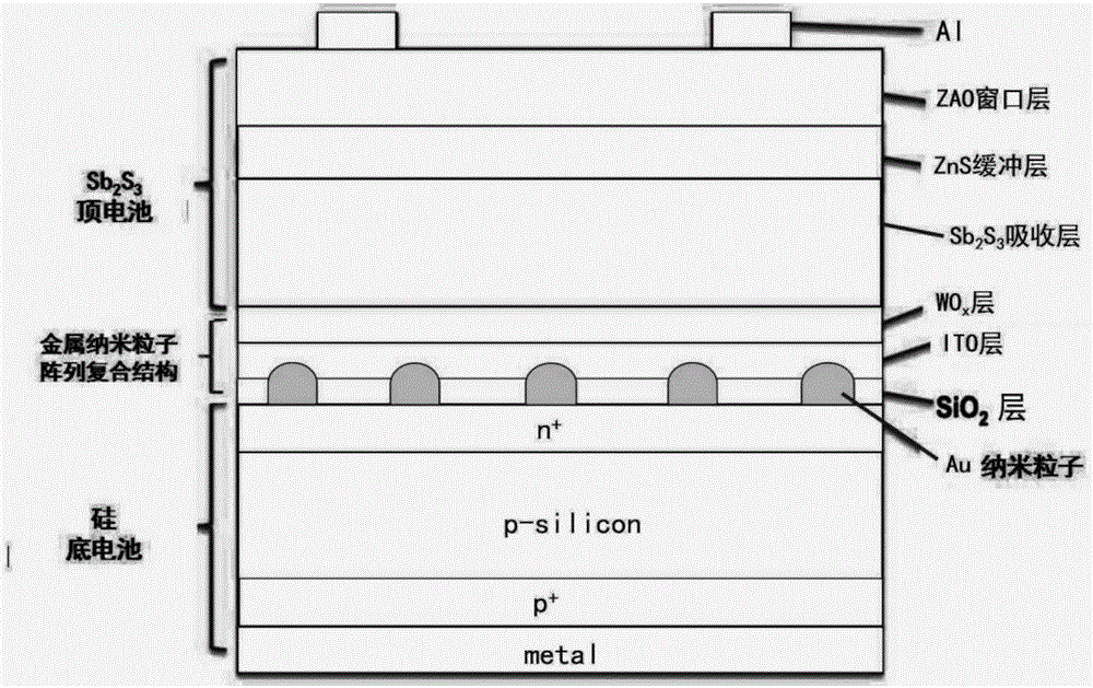
[0060] On the upper surface of the crystalline silicon cell that has not undergone texturing, passivation and metallization, an Au metal layer is prepared by vacuum evaporation. Using Au as the evaporation source, the air pressure is 0.001Pa, the evaporation source temperature is 800°C, and the evaporation time is 40min to form an Au metal layer with a thickness of about 30nm.

[0061] The Au metal layer is thermally annealed at 850° C. for 20 minutes in an argon atmosphere of 0.001 Pa to form an array of Au nanoparticles.

[0062] The ITO layer was prepared by magnetron sputtering, the substrate temperature was normal temperature, the sputtering power was 60w, the air pressure was 0.4Pa, and the sputtering time was 10min to form an ITO layer with a thickness of about 300nm.

[0063] Thermal annealing of the ITO layer makes it react with the surface of the silicon cell to form SiO 2 layer, the annealing temperature is 300°C, and the annealing time is 100min.

[0064] Prepara...

Embodiment 3

[0072] A Pd metal layer was prepared by magnetron sputtering on the upper surface of the crystalline silicon cell without texturing, passivation and metallization. Using Pd as the target material, DC sputtering is adopted, the sputtering power is 60w, the air pressure is 1.5Pa, the substrate temperature is normal temperature, the distance between the target and the substrate is 10cm, and the sputtering time is 15min to form a Pt metal layer with a thickness of about 150nm.

[0073] Thermally anneal the Pd metal layer at 300°C, 5×10 -4 Annealed in Pa argon atmosphere for 80min to form Pd nanoparticle array.

[0074] The FTO layer was prepared by magnetron sputtering. The substrate temperature is room temperature, the sputtering power is 80w, the air pressure is 1Pa, and the sputtering time is 15min, to form an FTO layer with a thickness of 800nm.

[0075] Thermally anneal the FTO layer to make it react with the surface of the silicon cell to form SiO 2 layer, the annealing t...


PUM

PropertyMeasurementUnit
Thicknessaaaaaaaaaa
Thicknessaaaaaaaaaa
Thicknessaaaaaaaaaa

Abstract

The invention discloses an antimony sulfide/silicon tandem solar cell and a preparation method thereof.The antimony sulfide/silicon tandem solar cell comprises a crystalline silicon bottom cell, an antimony sulfide thin-film top cell and a middle composite connection structure layer, wherein the middle composite connection structure layer comprises a silicon dioxide passivated layer, a TCO (transparent conductive oxide) layer and a high-work-function transition metal oxide layer sequentially from bottom to top, and the silicon dioxide passivated layer contains a metal nanoparticle array.The preparation method includes preparing the metal nanoparticle array, the silicon dioxide passivated layer, the TCO layer and the high-work-function transition metal oxide layer on the surface of the crystalline silicon cell sequentially; preparing the antimony sulfide thin-film solar cell on the surface of the transition metal oxide layer.The preparation method of the antimony sulfide/silicon tandem solar cell is less in material consumption, low in cost, capable of applying existing mature technologies and equipment to production and beneficial to popularization and application of the production technologies.

Description

technical field [0001] The invention relates to a stacked solar cell, in particular to an antimony sulfide / silicon stacked solar cell and a preparation method thereof, belonging to the field of solar cell materials and devices. Background technique [0002] As an important photoelectric energy conversion device, solar cells have developed rapidly in recent years due to their safety, pollution-free, simple maintenance, inexhaustible resources and long service life. Tandem solar cells belong to the third generation of solar cells. It can broaden the absorption spectrum of solar cells, convert light energy into electrical energy to the maximum extent, and improve the theoretical photoelectric conversion efficiency of solar cells. It is an important direction for the development of solar cells. [0003] Due to the wide energy distribution of the sunlight spectrum, any existing semiconductor material can only absorb photons with energy higher than its forbidden band width, and th...

Claims


Application Information

Patent Timeline
IPC IPC(8): H01L31/078H01L31/18
CPCH01L31/078H01L31/18Y02E10/50Y02P70/50
Inventor 刘芳洋陈鑫蒋良兴
Owner 湖南铱太科技有限公司
Why Eureka
Try Eureka