
A kind of preparation method of crystalline silicon and crystalline silicon

A technology of crystalline silicon and Czochralski monocrystalline silicon, applied in the field of solar cell materials, can solve the problems of low minority carrier lifetime and low yield of crystalline silicon, and achieve high minority carrier lifetime, high resistance pass rate, and high resistivity pass area. Effect

Active Publication Date: 2018-01-09
JIANGXI SAI WEI LDK SOLAR HI TECH CO LTD
View PDF8 Cites 0 Cited by
  • Summary
  • Abstract
  • Description
  • Claims
  • Application Information

AI Technical Summary

Problems solved by technology

[0006] In view of this, the present invention provides a method for preparing crystalline silicon containing boron and indium doping elements, which is used to solve the problem of low minority carrier lifetime and low yield of crystalline silicon in crystalline silicon co-doped with boron and gallium in the prior art. low problem

Method used


Image

  • A kind of preparation method of crystalline silicon and crystalline silicon
  • A kind of preparation method of crystalline silicon and crystalline silicon
  • A kind of preparation method of crystalline silicon and crystalline silicon

Examples


Embodiment 1

[0046] A preparation method of boron indium germanium co-doped polysilicon, comprising the following steps:

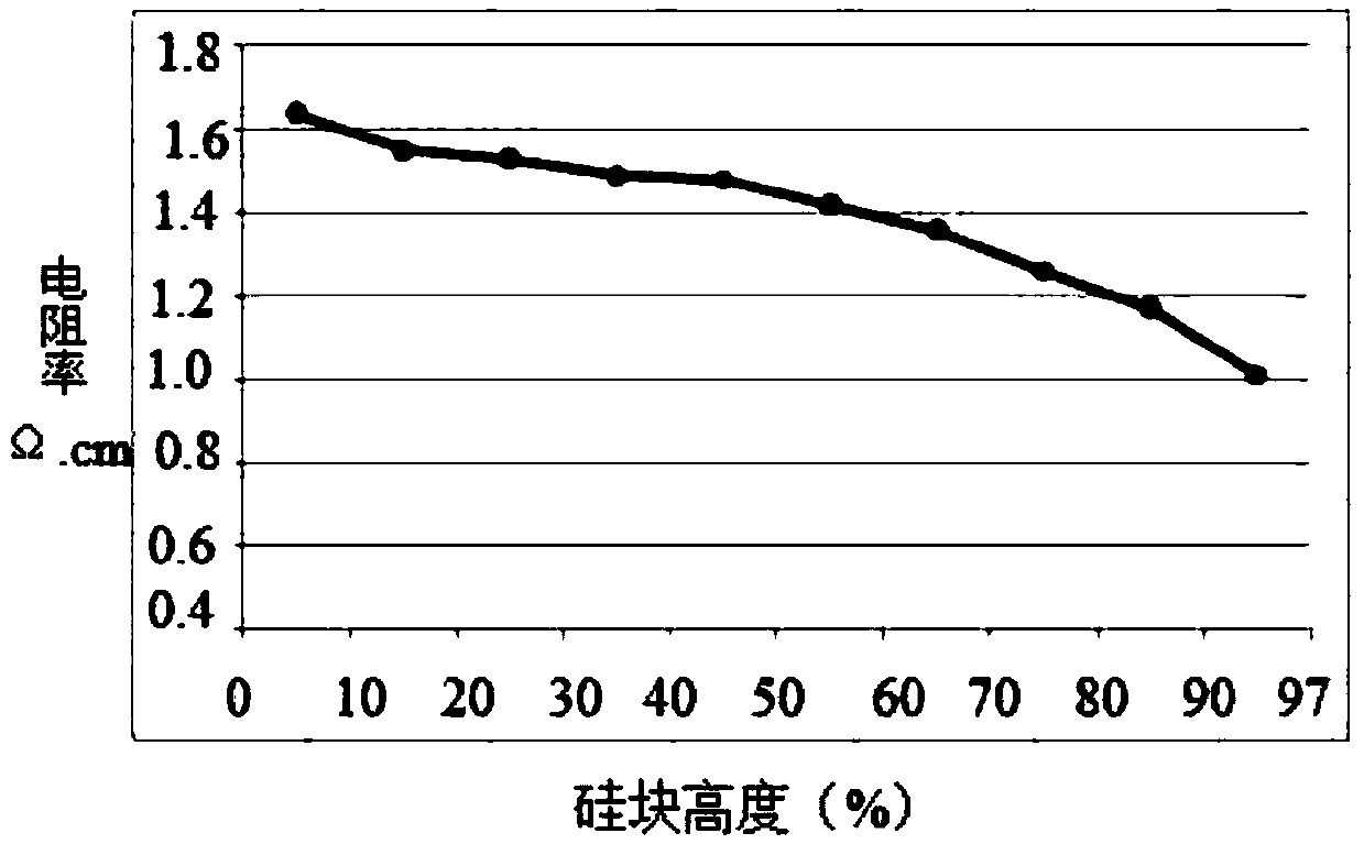
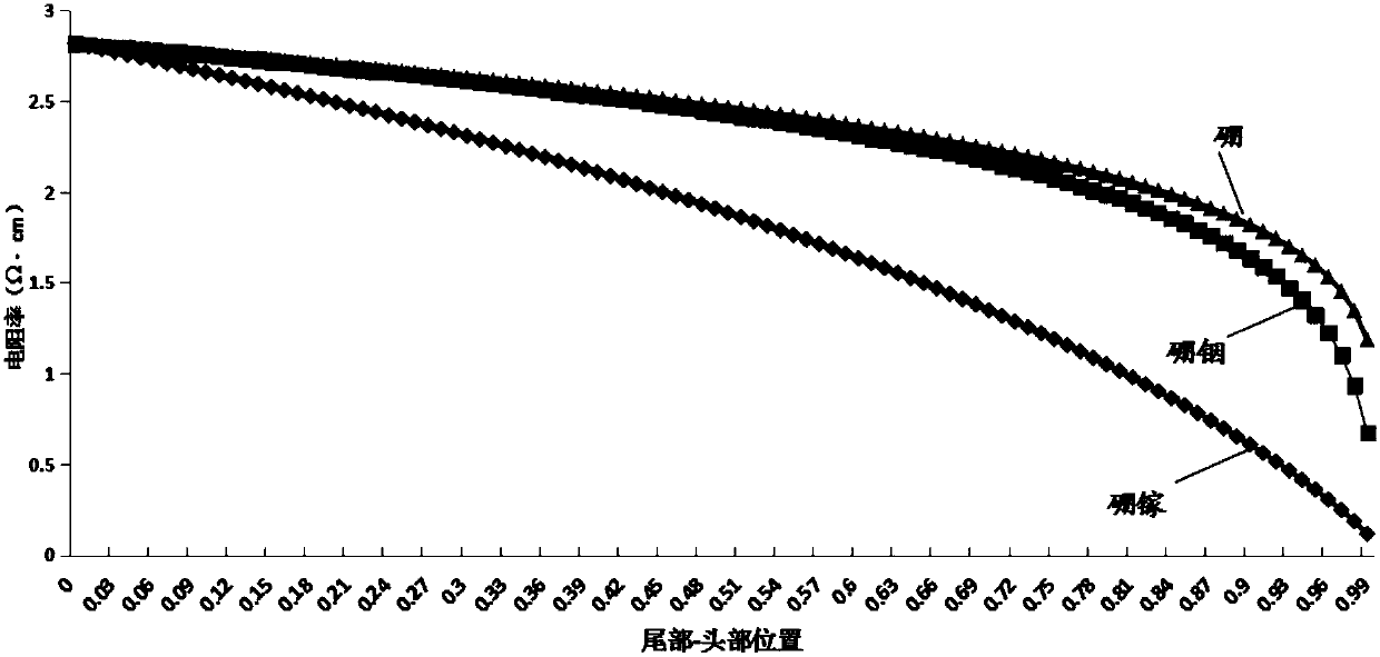
[0047] 1. Put 450kg of primary polysilicon material in a ceramic crucible, and simultaneously dope pure metal indium and pure metal germanium at 1 / 3 of the height of the crucible, wherein the masses of metal indium and metal germanium are 5g and 20g respectively, of which The atomic volume concentrations of In and Ge in the silicon material are 1.36E+17, 8.58E+10 respectively 17 atmos / cm 3 ; At 2 / 3 of the crucible height, add 60g of boron master alloy with a resistivity of 0.0026Ω.cm (in the boron master alloy, the atomic concentration of boron is 4.242E+19, the atomic volume concentration of B in the silicon material 6.52094E+15atmos / cm 3 ), so that the resistivity at 10% of the tail of the first grown polysilicon ingot is 2.78Ω·cm;

[0048] 2. Put the ceramic crucible with the above silicon material into the ingot furnace, evacuate the ingot furnace, check for lea...

Embodiment 2

[0056] A preparation method of boron indium germanium co-doped polysilicon, comprising the following steps:

[0057] 1. Put 500kg of primary polysilicon material in a ceramic crucible, and dope indium-silicon alloy and germanium-silicon alloy at the same time at 1 / 3 of the height of the crucible. Among them, the resistivity of indium-silicon alloy is 0.00002Ω·cm, and the mass is 35g. The content of indium in the alloy is 6.07E+21; the quality of the germanium-silicon alloy is 60g (the mass ratio of germanium and silicon in the germanium-silicon alloy is 1:1), wherein the atoms of In and Ge in the silicon material The volume concentration is 4E+17, 1.2E+17atmos / cm 3 , add boron powder 0.038g at 1 / 2 place of crucible height (the atomic volume concentration of B in described silicon material is 1.07E+16atmos / cm 3 ), so that the resistivity at the tail 10% of the first grown polysilicon ingot is 1.63Ω·cm;

[0058] Steps 2-3 are the same as in Embodiment 1.

[0059] Different pa...

Embodiment 3

[0062] A method for preparing a quasi-single crystal silicon ingot co-doped with boron, indium and germanium, comprising the following steps:

[0063] 1. Lay the bulk single crystal seed crystal (the crystal orientation is (100), the size is 156*156) on the bottom of the ceramic crucible, and the thickness of the seed crystal is between 10-30mm;

[0064] 2. Add 450kg of primary polysilicon material on top of the laid seed crystal, and dope pure indium and pure germanium with a weight of 50g and 100g respectively at 1 / 2 of the height of the crucible, wherein In and Ge are contained in the silicon material. Atomic volume concentrations are 1.3E+18, 4.3E+18atmos / cm 3 Doping 70g of boron master alloy at 3 / 5 of crucible height (the resistivity of boron master alloy is 0.0026, and the atomic volume concentration of B in the silicon material is 7.4E+15atmos / cm 3 ), so that the resistivity at the tail 10% of the first grown quasi-single crystal silicon ingot is 2.21Ω·cm;

[0065] 3....


PUM

PropertyMeasurementUnit
electrical resistivityaaaaaaaaaa
thicknessaaaaaaaaaa
sizeaaaaaaaaaa

Abstract

The invention provides a preparation method of crystalline silicon. The preparation method comprises the following steps: charging a silicon material into a crucible for growing crystalline silicon, at the same time putting doping agents into the crucible, putting the crucible into a furnace for growing the crystalline silicon, wherein the doping agents comprise a boron doping agent and an indium doping agent; the boron doping agent is one or more of a single substance, an alloy and nitride containing the boron element; the indium doping agent is one or more of a single substance, an alloy and nitride containing the indium element; the atomic volume concentration of the boron element and the indium element in a silicon material are respectively 10<14>-10<17>atmos / cm<3> and 10<14>-10<18>atmos / cm<3>; in the presence of a protecting atmosphere, heating to completely melt the silicon material and the doping agents in the crucible so as to obtain silicon melt, adjusting the crystalline silicon growth parameters, and enabling the silicon melt to grow crystal, thereby obtaining the crystalline silicon. By adopting the preparation method, the problems that in the prior art molecules of crystalline silicon prepared through boron-gallium codoping are short in service life and the crystalline silicon yield is relatively low are solved. The invention further provides the crystalline silicon.

Description

technical field [0001] The invention relates to the technical field of solar cell materials, in particular to a method for preparing crystalline silicon and crystalline silicon. Background technique [0002] Among all kinds of solar cells in the photovoltaic industry, crystalline silicon (monocrystalline silicon, polycrystalline silicon) solar cells occupy an extremely important position, and currently occupy more than 75% of the photovoltaic market. Most of the silicon wafer materials for the production of polycrystalline silicon solar cells are made of polycrystalline silicon ingots or processed from Czochralski silicon single crystals. [0003] In order to meet the requirements of cell processing, the required electrical properties must be obtained by adjusting the concentration of dopants during the growth of crystalline silicon. The existing dopants include group III elements boron and gallium (to prepare P-type silicon wafers) and group V element phosphorus (to prepar...

Claims


Application Information

Patent Timeline
Patent Type & Authority Patents(China)
IPC IPC(8): C30B29/06C30B15/04C30B11/04C30B28/06
CPCC30B11/04C30B15/04C30B28/06C30B29/06
Inventor 罗鸿志胡动力何亮
Owner JIANGXI SAI WEI LDK SOLAR HI TECH CO LTD
Learn More