Bismuth telluride based N type thermoelectric material and preparation method thereof
A thermoelectric material, bismuth telluride technology, applied in the direction of thermoelectric device junction lead-out material, thermoelectric device manufacturing/processing, etc., can solve the development limitation of nano-Bi2Te3-based thermoelectric materials, difficult to form large-scale industrial applications, nanostructures It is easy to be damaged and other problems, and achieves the effect of outstanding thermoelectric performance, improved Seebeck coefficient and high density.
- Summary
- Abstract
- Description
- Claims
- Application Information
AI Technical Summary
Problems solved by technology
Method used
Image
Examples
Embodiment 1
[0021] The optional elemental raw materials can be selected according to Bi 2 (Te 0.92 Se 0.08 ) 3 , chemical formula content weighing, where Te is 500 grams, the Bi content can be increased by 0.4% by weight on the basis of the normal stoichiometric ratio; metal antimony (Sb) and the weight percentage of 0.02% by weight are added on the basis of the stated weight 0.03% non-metallic iodine (I), the purity of all elemental raw materials is above 4N;
[0022] Put the above-mentioned weighed materials into the sintered flat quartz tube at the bottom, vacuumize and seal the tube, then put it into a resistance-heated swing furnace, place the quartz tube vertically, and react at 800 °C for 12 hours. Swing the furnace body, ① the swing frequency is controlled at 0.04Hz, and the swing time is determined by the fluctuation of the furnace field temperature from the beginning of swing until the temperature indication value is constant; ② the interval between two adjacent swings is 50 ...
Embodiment 2
[0024] Cut and polished samples (Bi 1-x Sb x ) 2 Te 3 Conduct thermoelectric performance tests. Prepared by the above method (Bi 1-x Sb x ) 2 Te 3 Block samples were cut with a wire cutter and sanded. The sample is first cut into basic discs and cuboid samples with a cutting machine, and then polished with sandpaper; the thickness of the disc sample is 2.0mm, and the diameter is 12.0mm. The cross-sectional area of the cuboid is 2.5 × 2.5 mm 2 , The thermal diffusivity of the wafer was tested on a NETZSCH LFA467 laser thermal conductivity meter, using pyrocream9606 as a standard sample, and tested under an argon atmosphere. The conductivity and Seebeck coefficient of the samples were tested on ULVAC ZEM-3.
Embodiment 3
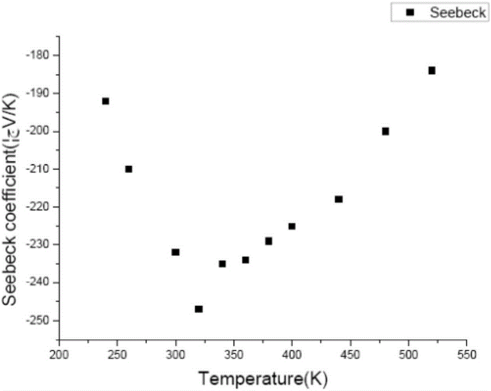
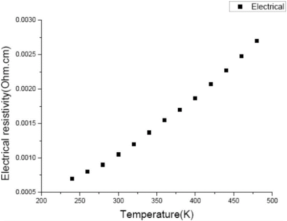
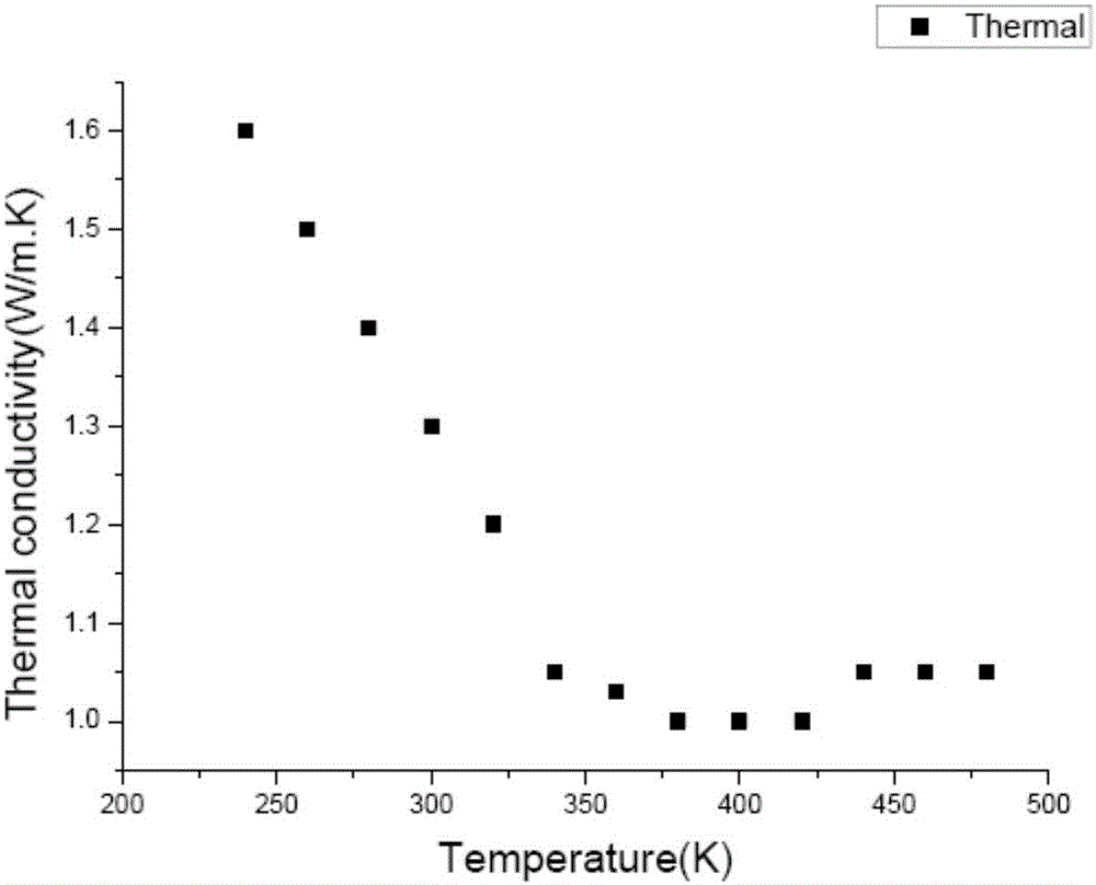
[0026] Sample (Bi 1-x Sb x ) 2 Te 3 The thermoelectric performance test results of
[0027] The above test results show that the resistivity increases with the increase of temperature, from 10.1*10 at room temperature -6 Ω m increased to 2.7*10 at 480K -5Ωm. The absolute value of the Seebeck coefficient first increases with the increase of temperature, reaches a maximum of 247μV / K at 320K, and then decreases. A positive Seebeck coefficient indicates that (Bi 1-x Sb x ) 2 Te 3 Most of the carriers are holes. The thermal conductivity becomes smaller as the temperature increases, and the thermal conductivity near room temperature is 1.3W / m.K. According to the figure of merit calculation formula of thermoelectric materials: Z=S 2 σ / K, where S is the Seebeck coefficient of the material, σ is the electrical conductivity, and K is the thermal conductivity, it can be obtained that (Bi 1-x Sb x ) 2 Te 3 The ZT value of the sample was 1.33 at 340K.
PUM
| Property | Measurement | Unit |
|---|---|---|
| Thickness | aaaaa | aaaaa |
| Diameter | aaaaa | aaaaa |
Abstract
Description
Claims
Application Information


