Holographic imaging film based on surface plasma coupling structure
A surface plasmon and coupling structure technology, applied in nanotechnology, instruments, etc., can solve problems such as image distortion, limit development, hinder the development and marketization of three-dimensional display holographic technology, achieve wide viewing angles, and improve reflection efficiency.
- Summary
- Abstract
- Description
- Claims
- Application Information
AI Technical Summary
Problems solved by technology
Method used
Image
Examples
Embodiment 1
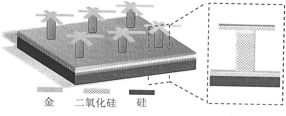
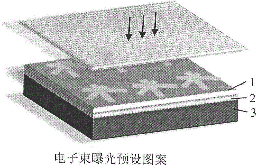
[0022] (1) thermal oxidation passivation layer: utilize thermal oxidation growth on the surface of silicon (Si) substrate 1 Thick SiO 2 as a passivation layer.
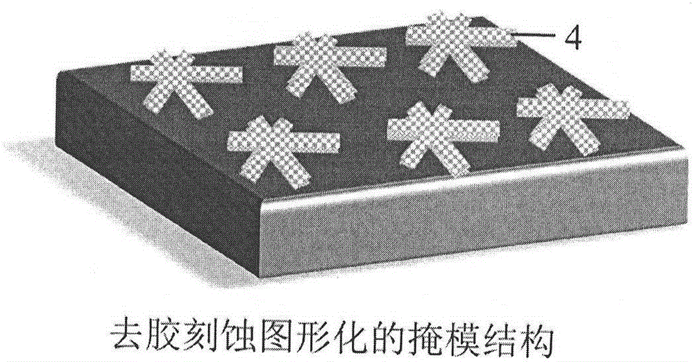
[0023] (2) Photolithographic patterning: Take AR-N7520.18 negative photoresist as an example, spin-coat it with a thickness of 100nm at a speed of 5000 rpm, and pre-bake it in an oven at 85°C for 5 minutes, using NanoBeam electronics The beam etching system exposes the photoresist with an accelerating voltage of 80kV, develops it in tetramethylammonium hydroxide (TMAH) developer solution for 1 minute, and rinses it with deionized water to obtain an imaged nanostructure array;
[0024] (3) Formation of insulating dielectric nanocolumns: use silicon oxide as a mask, etch the silicon substrate with a reactive ion etching machine, the power of the etching machine is 400W, SF 6 and C 4 f 8 The flow rates were 40 and 90 sccm / min, the etching time was 50 seconds, and SF 6 As an etching gas, C 4 f 6 As the polymer gen...
PUM
 Abstract
Description
Claims
Application Information


