A Method for Optimizing CMOS Image Sensor Wafer Edge Defects

An image sensor, edge defect technology, used in semiconductor/solid-state device manufacturing, electrical components, circuits, etc., can solve problems such as inability to grow silicon nitride, affecting yield, and online defects

Active Publication Date: 2018-08-24
SHANGHAI HUALI MICROELECTRONICS CORP
View PDF3 Cites 0 Cited by
  • Summary
  • Abstract
  • Description
  • Claims
  • Application Information

AI Technical Summary

Problems solved by technology

However, due to the inherent characteristics of furnace tube growth, three 20*20mm support points P1, P2 and P3 (indicated by dotted lines in the figure) are generally required to support the wafer (such as figure 1 As shown), these three points are in close contact with the three edge regions on the back of the wafer, and silicon nitride cannot be grown, resulting in the exposure of the low-temperature oxide at the three edge regions on the back of the wafer to etching in subsequent etching. In the plasma
The low-temperature oxide material on the back side is loose, and it is easy to be bombarded by the plasma to produce silicon oxide particles. Under the flow of cooling helium gas on the back side of the wafer, it will be driven and dropped on the edge surface of the wafer, causing online defects and affecting the yield.

Method used


Image

  • A Method for Optimizing CMOS Image Sensor Wafer Edge Defects
  • A Method for Optimizing CMOS Image Sensor Wafer Edge Defects

Examples


Embodiment Construction

[0026] In order to make the content of the present invention clearer and easier to understand, the content of the present invention will be described in detail below in conjunction with specific embodiments and accompanying drawings.

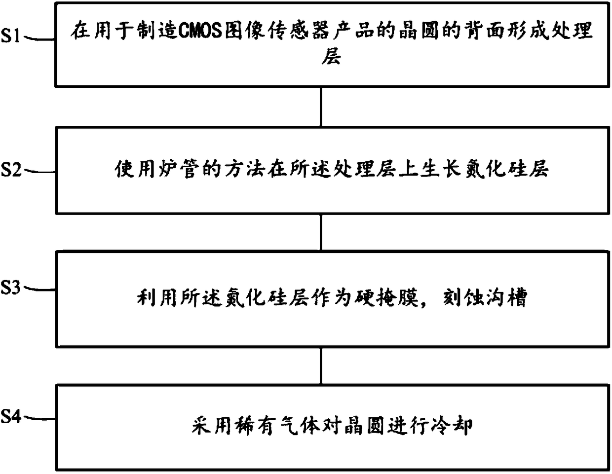
[0027] In the present invention, by changing the material of the low-temperature oxide on the back of the CMOS image sensor wafer to prevent metal contamination and reduce signal noise interference, it is optimized to a denser plasma-assisted oxide (PEOX, Plasma Enhanced Oxide) or chemical vapor phase Deposit nitride or a combination of these two films to prevent the small-sized low-temperature oxide silicon oxide particles produced by plasma bombardment on the back of the wafer during the shallow trench etching process from cooling the helium gas on the back of the wafer. The movement causes etch defects on the front side of the wafer. The invention greatly reduces online defects and improves product yield through optimization.

[0028] Prefer...


PUM


Abstract

The invention provides a method of optimizing the wafer edge defect of a CMOS image sensor, comprising the following steps: S1, forming a processing layer on the back of a wafer for manufacturing a CMOS image sensor product, wherein the processing layer includes a plasma-enhanced oxide layer, a chemical vapor deposition nitride layer, or a combination of the plasma-enhanced oxide layer and the chemical vapor deposition nitride layer; S2, growing a silicon nitride layer on the processing layer using a furnace tube; and S3, using the silicon nitride layer as a hard mask to etch a trench.

Description

technical field [0001] The invention relates to the field of semiconductor manufacturing, and more specifically, the invention relates to a method for optimizing the edge defects of a CMOS image sensor wafer. Background technique [0002] CIS (CMOS Image Sensor, CMOS image sensing device) is a photoelectric conversion device, which adopts a column of built-in LED (Light Emitting Diode, light emitting diode) for illumination. Due to the small size and light weight of this CMOS sensor, it is widely used in mobile devices such as smartphones with camera functions. [0003] The imaging function of this CMOS sensor is particularly sensitive to metal pollution, especially the increase in leakage and white spots caused by pollution in the work area, resulting in low yield and even scrapping a large number of wafers. [0004] In order to prevent metal ion contamination on the back of the wafer during the process, a layer of silicon oxide is usually grown on the back of the CMOS ima...

Claims


Application Information

Patent Timeline
Patent Type & Authority Patents(China)
IPC IPC(8): H01L21/306
CPCH01L21/306
Inventor 冯奇艳许进唐在峰任昱吕煜坤
Owner SHANGHAI HUALI MICROELECTRONICS CORP
Why Eureka
Try Eureka