Flash memory device and manufacturing method thereof

A flash memory device and manufacturing method technology, applied in semiconductor/solid-state device manufacturing, semiconductor devices, electric solid-state devices, etc., can solve the problems of programming interference, low programming efficiency, etc., to prevent leakage current, good corrosion resistance, increase Effects of programming or programming disturbance tolerance

Active Publication Date: 2019-03-08
SHANGHAI HUAHONG GRACE SEMICON MFG CORP
View PDF4 Cites 0 Cited by
  • Summary
  • Abstract
  • Description
  • Claims
  • Application Information

AI Technical Summary

Problems solved by technology

[0005] The purpose of the present invention is to provide a flash memory device and its manufacturing method, which can solve the problem of low programming efficiency or programming interference caused by shallow trench isolation structure groove defects

Method used


Image

  • Flash memory device and manufacturing method thereof
  • Flash memory device and manufacturing method thereof
  • Flash memory device and manufacturing method thereof

Examples


Embodiment Construction

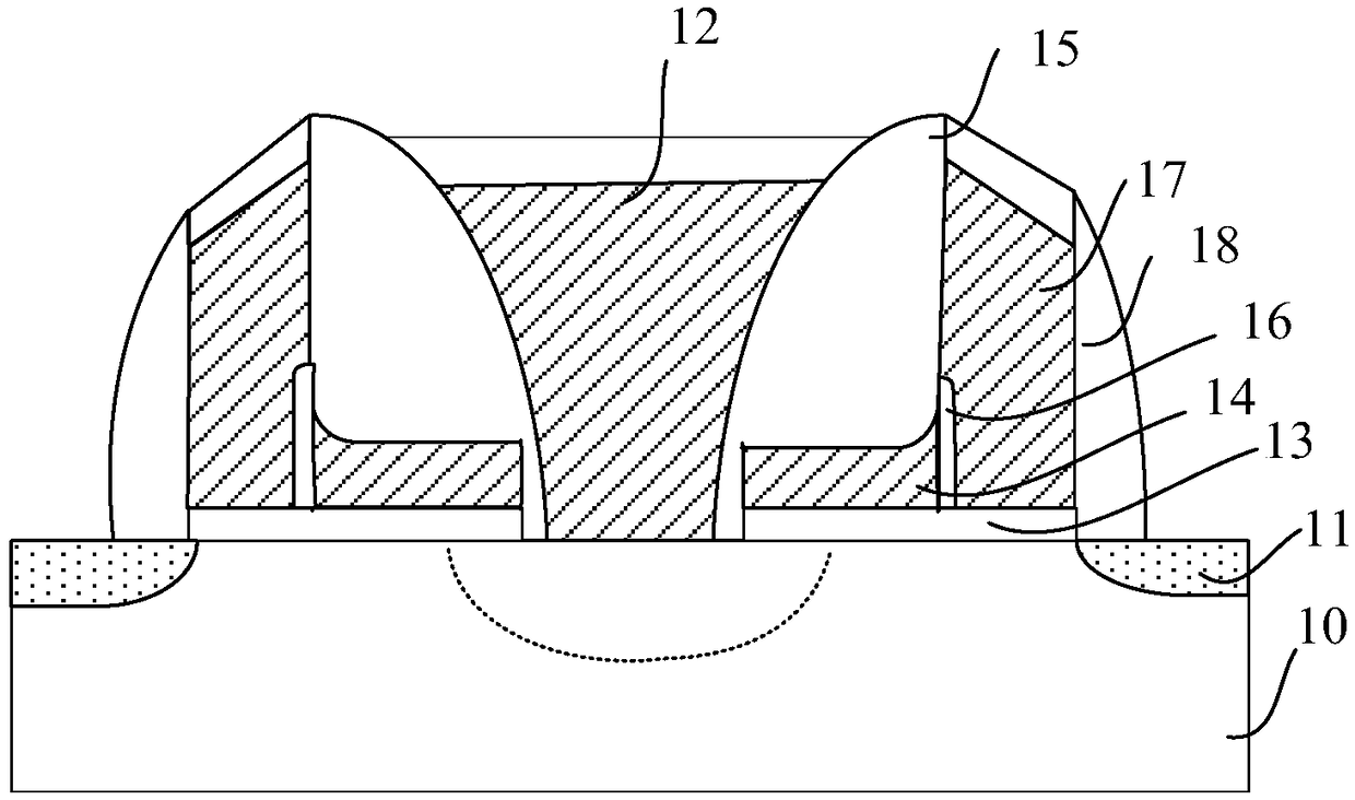
[0037] In order to make the purpose and features of the present invention more obvious and understandable, the specific implementation of the present invention will be further described below in conjunction with the accompanying drawings. However, the present invention can be implemented in different forms and should not be limited to the described embodiments.

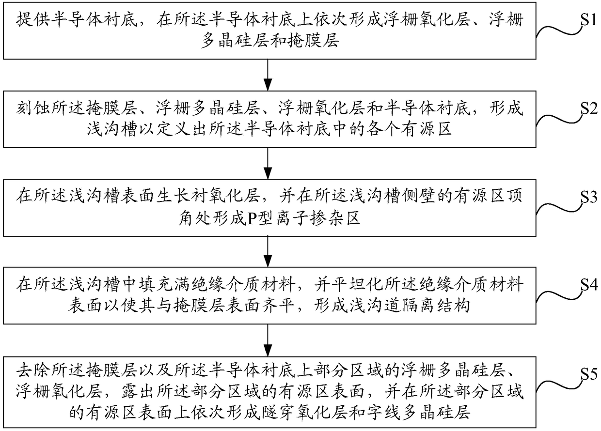
[0038] Please refer to figure 2 , the present invention proposes a kind of manufacturing method of flash memory device, comprises the following steps:

[0039] S1, providing a semiconductor substrate, and sequentially forming a floating gate oxide layer, a floating gate polysilicon layer and a mask layer on the semiconductor substrate;

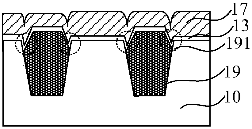
[0040] S2, etching the mask layer, the floating gate polysilicon layer, the floating gate oxide layer and the semiconductor substrate to form shallow trenches to define each active region in the semiconductor substrate;

[0041] S3, growing a liner oxide layer (Liner oxide) on the s...


PUM


Abstract

The invention provides a flash memory device and a manufacturing method thereof. After the lining oxide layer is formed on the side wall of the shallow trench, P-type ion implantation is performed on the top corner of the active region of the side wall of the shallow trench to form P-type ion doping. area, to effectively improve the density of the liner oxide layer on the sidewall of the shallow trench, and to make the active area and the top boundary of the shallow trench isolation structure amorphized, with good corrosion resistance, which greatly reduces the impact of subsequent processes on the active area and the shallow trench isolation structure. The loss at the top of the top boundary of the shallow trench isolation structure reduces the depth of the pit at the top of the shallow trench isolation structure, reduces the distortion of the word line polysilicon layer formed subsequently and increases its height, and improves the narrow width effect. The off-state leakage current of the subsequently formed word line transistor is reduced and the threshold voltage thereof is increased, thereby increasing the program or program disturbance tolerance of the flash memory device. At the same time, the reliability and insulation of the subsequently formed shallow trench isolation structure are improved, and electric leakage of the shallow trench isolation structure is effectively prevented.

Description

technical field [0001] The invention relates to the field of semiconductor manufacturing, in particular to a flash memory device and a manufacturing method thereof. Background technique [0002] Generally speaking, flash memory includes two basic structures: gate stack (stackgate) and split gate (splitgate) structure. Please refer to Figure 1A , the existing structure of a split-gate flash memory unit includes: a semiconductor substrate 10; a drain region (ie bit line, BL) 11 located in the substrate of the semiconductor substrate 10; a source line located on the surface of the semiconductor substrate 10 Polysilicon layer (i.e. source line, SL) 12; floating gate oxide layer 13 and floating gate 14 located on the surface of semiconductor substrate 10 on both sides of the source line polysilicon layer 12; The oxide layer (Tunnel Oxide) 13, the side wall dielectric layer 15 between the floating gate 14; the tunnel oxide layer 16, the word line polysilicon layer located on the...

Claims


Application Information

Patent Timeline
Patent Type & Authority Patents(China)
IPC IPC(8): H01L21/265H01L27/11517
CPCH01L21/26586H10B41/00
Inventor 王卉曹子贵陈宏徐涛
Owner SHANGHAI HUAHONG GRACE SEMICON MFG CORP
Why Eureka
Try Eureka