Thermally-assisted field electron emission cathode structure and preparation method thereof

A field electron emission, cathode structure technology, applied in cold cathode manufacturing, electrode system manufacturing, discharge tube/lamp manufacturing, etc. The effect of simplicity, improved performance, wide application value

Active Publication Date: 2016-08-17
SUN YAT SEN UNIV
View PDF4 Cites 8 Cited by
  • Summary
  • Abstract
  • Description
  • Claims
  • Application Information

AI Technical Summary

Problems solved by technology

However, the existing heat-assisted field emission electron sources all need to apply an additional bias voltage on the heating filament to generate Joule heat, which consumes a lot of power, and the cathode structure is relatively complicated, making it difficult to manufacture an array type electron source.

Method used


Image

  • Thermally-assisted field electron emission cathode structure and preparation method thereof
  • Thermally-assisted field electron emission cathode structure and preparation method thereof
  • Thermally-assisted field electron emission cathode structure and preparation method thereof

Examples


Embodiment 1

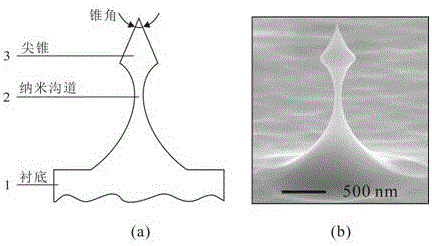
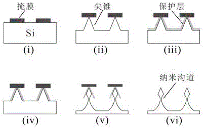
[0038] A preparation of a heat-assisted field electron emission cathode structure (the diameter or width of the narrowest part of the nanochannel is about 100 nm, and the corresponding resistance value is about 100 kΩ), including the following steps:

[0039] S1. On a clean silicon substrate, use a chemical vapor deposition system to deposit a silicon dioxide / silicon nitride mask layer with a thickness of 500-1000 nm on its surface;

[0040]S2. Spin-coat a photoresist (AR-N 7520) with a thickness of about 500-600 nm; use an electron beam lithography system to expose the photoresist; develop the exposed sample to obtain a center-to-center distance of 6 μm Circular or strip-shaped photoresist array, the diameter or width of the circle or strip can be 700-1500 nm;

[0041] S3. Use the plasma reactive etching system to etch the silicon dioxide / silicon nitride not protected by the photoresist until the silicon substrate is exposed, leaving the silicon dioxide / silicon nitride protec...

Embodiment 2

[0048] The experimental method is the same as that in Example 1, the only difference is that on the basis of preparing an emitter with a diameter or width of about 100 nm in the narrowest part of the nanochannel in S8, an additional step is added:

[0049] S81. Oxidize the sample obtained in S8 in an oxygen atmosphere at 900 °C for 50 min (the oxygen flow rate is 0.9 SLM), so that the diameter or width of the narrowest part of the nanochannel is reduced to about 70 nm (the corresponding resistance value is about is 1 MΩ), and the surface oxide layer was removed with a mixed solution of deionized water and hydrofluoric acid with a volume ratio of 5:1.

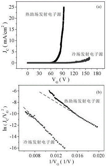
[0050] A silicon emitter array (40 × 40) with a diameter of about 70 nm in the narrowest part of the nanochannel was prepared using the above process. As a comparison, the inventors also fabricated a conventional nanochannel-free silicon tip array (40×40). The spacing between emitters in the array was all 6 μm. The gate is int...

Embodiment 3

[0052] The experimental method is the same as in Example 1, the only difference is that step S1 directly selects a substrate covered with 300 nm of silicon dioxide, or directly selects a substrate covered with 100 nm of alumina.


PUM


Abstract

The invention discloses a thermally-assisted field electron emission cathode structure and a preparation method thereof. The cathode structure is perpendicular to the surface of a substrate and is composed of a pointed cone at the top and a nano-channel in the bottom. The cone angle of the pointed cone is 15-60 degrees, and the diameter or width of the narrowest part of the nano-channel is 10-100 nm. When the cathode structure works, the nano-channel limits conduction of Joule heat generated by the pointed cone in the field emission process, so that the temperature of the pointed cone is increased, thermally-assisted field emission is achieved, and electron emission performance is improved; due to the negative feedback current limiting effect of the resistance of the nano-channel, overcurrent breakdown of an emitter can be avoided; due to the heat capacity of the pointed cone, it can be avoided that the pointed cone is melted due to too high temperature of the pointed cone. According to the cathode structure, self-heating of the emitter can be achieved, cathode failures caused by high temperature and large current can be avoided, and application of the cathode in low-voltage driving and high-stability electron sources is prompted. The cathode structure does not need heating filaments and is simple in structure, and array electron sources can be easily manufactured.

Description

technical field [0001] The invention relates to the technical field of nanometer electronic devices, in particular to a heat-assisted field electron emission cathode structure and a preparation method thereof. Background technique [0002] The field emission electron source has the characteristics of low working temperature, low power consumption and fast response speed. devices with potential applications. When the electron source is working, the change of the work function caused by the adsorption on the surface of the cathode; the difference in the local electric field of each emitting end surface caused by the difference in the geometry of the emitters in the array will affect the current stability and reliability of the field emission electron source. The above problems limit the application development of field emission electron sources. Thermally assisted field emission electron sources are mostly used in commercial electron sources at present. In conventional heat...

Claims


Application Information

Patent Timeline
Patent Type & Authority Applications(China)
IPC IPC(8): H01J1/304H01J9/02
CPCH01J1/3044H01J9/025
Inventor 佘峻聪黄志骏邓少芝许宁生陈军
Owner SUN YAT SEN UNIV
Why Eureka
Try Eureka