Flexible full-transparent amorphous oxide thin film transistor and preparation method thereof
A technology of amorphous oxide and oxide thin film, which is applied in transistors, semiconductor/solid-state device manufacturing, semiconductor devices, etc., can solve the problems of low resistivity, poor stability of devices, high resistivity, etc., and achieve good electrical properties, high The effect of visible light transmittance
- Summary
- Abstract
- Description
- Claims
- Application Information
AI Technical Summary
Problems solved by technology
Method used
Image
Examples
Embodiment 1
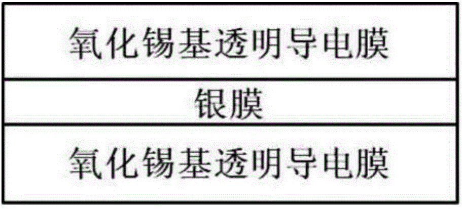
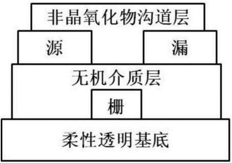
[0037] Using PET as the substrate, amorphous indium gallium zinc oxide (In-Ga-Zn-O) film as the channel layer, inorganic Al 2 o 3 The thin film is used as the dielectric layer, the ITO thin film is used as the gate electrode layer, and the molybdenum (Mo)-doped SnO 2 A silver-based transparent conductive multilayer film composed of transparent conductive oxide and silver film (SnO 2 : Mo / Ag / SnO 2 : Mo) as the source / drain electrode layer, the structure of the silver-based transparent conductive multilayer film is as figure 1 As shown, a flexible fully transparent amorphous oxide TFT with a bottom gate coplanar structure is prepared, and the structure of the flexible fully transparent amorphous oxide TFT is as follows figure 2 As shown, the specific steps are as follows:
[0038] (1) Use radio frequency magnetron sputtering method on the PET substrate to form an ITO film with a thickness of 80nm with the aid of an aluminum oxide mask. The target material is an ITO ceramic ...
Embodiment 2
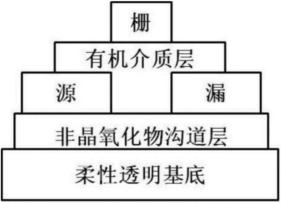
[0044] Using PET as the substrate, amorphous indium gallium zinc oxide (In-Ga-Zn-O) film as the channel layer, organic PMMA film as the dielectric layer, ITO film as the gate electrode layer, molybdenum (Mo) SnO 2 A silver-based transparent conductive multilayer film composed of transparent conductive oxide and silver film (SnO 2 : Mo / Ag / SnO 2 : Mo) as the source / drain electrode layer, the structure of the silver-based transparent conductive multilayer film is as figure 1 As shown, a flexible fully transparent amorphous oxide TFT with a coplanar top gate structure is prepared, and the structure of the flexible fully transparent amorphous oxide TFT is as follows image 3 As shown, the specific steps are as follows:
[0045] (1) An amorphous indium gallium zinc oxide film with a thickness of 50nm is formed on a PET substrate by radio frequency magnetron sputtering. The target material is an indium gallium zinc oxide target with a purity of 4N. The sputtering power is 20W and ...
PUM
| Property | Measurement | Unit |
|---|---|---|
| thickness | aaaaa | aaaaa |
| thickness | aaaaa | aaaaa |
| thickness | aaaaa | aaaaa |
Abstract
Description
Claims
Application Information


