

Efficient perovskite monocrystal light detector and preparation method thereof
A photodetector and perovskite technology, applied in the field of photodetectors, can solve the problems of short lifespan, unstable working state, low performance of polycrystalline perovskite thin film photodetectors, etc., and achieve low production cost and low defects. The effect of density of states, excellent thermal stability
- Summary
- Abstract
- Description
- Claims
- Application Information
AI Technical Summary
Problems solved by technology
Method used
Image

Examples
preparation example Construction
[0029] The invention provides a high-efficiency perovskite single-crystal photodetector, and also relates to a preparation method of the detector. The specific preparation method includes the following steps:
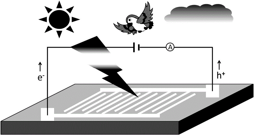
[0030] A high-efficiency perovskite single crystal photodetector comprises a perovskite single crystal and interdigitated electrodes arranged on the perovskite single crystal. Perovskite single crystals with ABX 3 Single crystal of perovskite structure, where A is CH 3 NH 3 + 、H 2 N-CH=NH 2 + , (CH 3 ) 4 N + 、C 7 h 7 + 、Cs + or C 3 h 11 SN 3 2+ ; B is Pb, Ge or Sn; X is Cl, Br or I.
[0031] The thickness of the interdigitated electrodes is 1nm-1cm, the finger width is 10nm-1cm, the spacing is 10nm-1cm, the finger length is 10nm-10cm, and the photosensitive area is 200nm 2 ~400cm 2; The interdigitated electrodes are metal or metal-containing alloy electrodes, such as silver (Ag), copper (Cu), gold (Au), aluminum (Al), sodium (Na), molybdenum (Mo), tun...
Embodiment 1
[0039] 1) Soak the cultivated perovskite single crystal with anhydrous ether to clean and remove the impurities remaining on the surface of the single crystal during the cultivation process;
[0040] 2) Polishing the cleaned single crystal surface, after polishing, use gas purging to remove fine particles such as powder remaining on the single crystal surface during the polishing process;
[0041] 3) Subsequently, the single crystal is placed in a vacuum drying oven to dry;
[0042] 4) Fix the metal mask plate with interdigitated pattern on the polished and cleaned perovskite single crystal side;
[0043] 5) Thermally evaporate and deposit interdigitated gold electrodes with a thickness of 1 nm, a finger width of 10 nm, a spacing of 10 nm, and a finger length of 10 nm on one side of the single crystal with a fixed mask;
[0044] 6) The prepared finished single crystal perovskite photodetector is sealed and packaged for testing.
Embodiment 2
[0046] 1) soaking the cultured perovskite single crystal with cyclohexane to clean and remove impurities remaining on the surface of the single crystal during the culture process;
[0047] 2) Polishing the cleaned single crystal surface, after polishing, use anhydrous ether ultrasonic cleaning to remove fine particles such as powder remaining on the single crystal surface during the polishing process;
[0048] 3) Subsequently, the single crystal is placed in a vacuum drying oven to dry;
[0049] 4) Fix the metal mask plate with interdigitated pattern on the polished and cleaned perovskite single crystal side;
[0050] 5) Magnetron sputtering on one side of the single wafer with the mask fixed has a thickness of 50nm, a finger width of 50nm, a spacing of 50nm, and an interdigital silver electrode with a finger length of 50nm;
[0051] 6) The prepared finished single crystal perovskite photodetector is sealed and packaged for testing.
PUM
| Property | Measurement | Unit |
|---|---|---|
| Thickness | aaaaa | aaaaa |
| Spacing | aaaaa | aaaaa |
Abstract
Description
Claims
Application Information