Silicon-based suspended microstrip line structure for terahertz waves, and manufacturing method therefor

A microstrip line and terahertz technology, applied in the field of microelectronics, can solve the problems of large volume, high cost, and high loss of microstrip line, and achieve the effects of high surface flatness, high structural strength, and good microwave performance

Inactive Publication Date: 2016-08-24
XIDIAN UNIV
View PDF4 Cites 9 Cited by
  • Summary
  • Abstract
  • Description
  • Claims
  • Application Information

AI Technical Summary

Problems solved by technology

[0005] The structure of the traditional suspended microstrip line generally requires a thicker dielectric substrate as the suspension layer of the microstrip line. When transmitting the terahertz band, the thickness of the dielectric substrate will be compared with the wavelength of the electromagnetic wave, which brings significant Dielectric loss, resulting in higher losses for suspended microstrip lines
In addition, the traditional suspended microstrip line structure also needs a metal box as a metal shielding cavity, which is expensive, large in size, high in quality, and low in precision.
Moreover, the small-sized standard microstrip line structure is difficult to achieve high-precision processing
[0006] The processing of traditional suspended microstrip lines generally uses materials such as microwave boards, plastics, ceramics, or silicon dioxide as suspension dielectric substrates. However, it is difficult to process microwave boards into thin-layer support structures, and plastics and ceramics are not easy to achieve sub-micron level. Accuracy, silicon dioxide may break during the growth process, there are many interface charges at the silicon dioxide and silicon interface, and the preparation of the metal box makes the traditional suspended microstrip line incompatible with the traditional IC process
In addition, when the operating frequency reaches the terahertz frequency band, it is difficult for the ordinary processing technology to realize the small size and high precision structure of the transmission line.
These factors not only increase the processing difficulty and processing cost, but also affect its performance and reliability

Method used


Image

  • Silicon-based suspended microstrip line structure for terahertz waves, and manufacturing method therefor
  • Silicon-based suspended microstrip line structure for terahertz waves, and manufacturing method therefor
  • Silicon-based suspended microstrip line structure for terahertz waves, and manufacturing method therefor

Examples


Embodiment 1

[0057] Example 1: Making a 50-ohm terahertz silicon-based suspended microstrip line

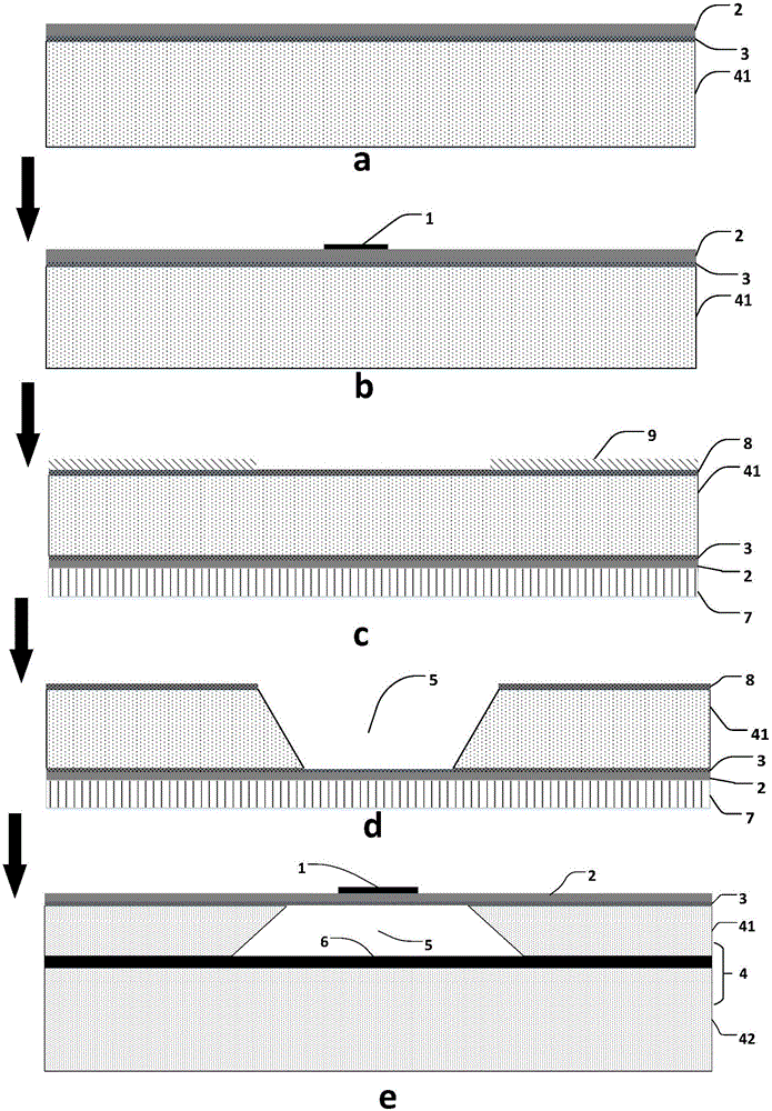
[0058] Step A, making a suspension layer of the microstrip line.

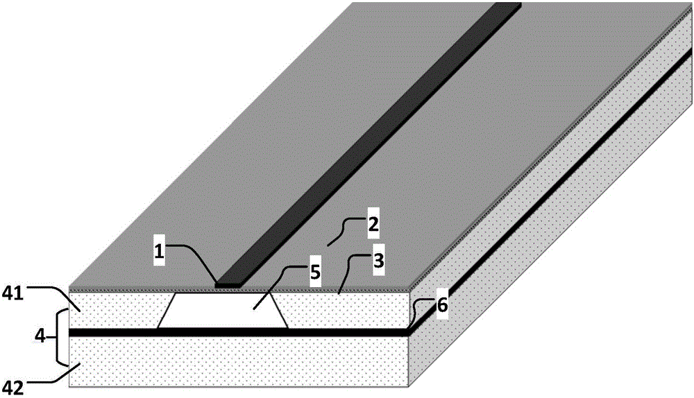
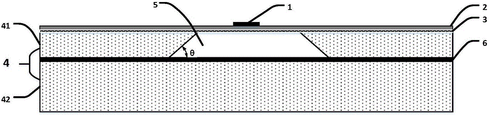
[0059] Get two silicon wafers of the same size as the upper silicon substrate 41 and the lower silicon substrate 42 respectively, and grow a 0.1 micron thick silicon nitride layer 3 on the upper surface of the upper silicon substrate 41; 3. Smear the adhesion promoter and BCB photoresist in sequence, and after exposure, it will be cured by self-heating to form a smooth and flat suspension layer with a thickness of 5 microns, such as image 3 as shown in a.

[0060] Step B, making microstrip lines.

[0061] B1) Deposit a layer of titanium Ti with a thickness of 8 nanometers on the suspension layer by evaporation or sputtering, and then deposit a layer of gold Au with a thickness of 92 nanometers on the titanium metal layer to form a plating layer for the microstrip line;

[0062] B2) smear a layer of 4 micron thick positive ...

Embodiment 2

[0077] Embodiment 2: Fabricate a 100-ohm terahertz silicon-based suspended microstrip line.

[0078] Step 1, making the suspension layer of the microstrip line.

[0079] Get two silicon wafers of the same size as the upper silicon substrate 41 and the lower silicon substrate 42 respectively, and grow a 0.2 micron thick silicon nitride layer 3 on the upper surface of the upper silicon substrate 41; 3. Smear the adhesion promoter and BCB photoresist in sequence, and after exposure, it will be cured by self-heating to form a smooth and flat suspension layer with a thickness of 4 microns, such as image 3 as shown in a.

[0080] Step 2, make the microstrip line.

[0081] 2.1) Deposit a layer of titanium Ti with a thickness of 6 nanometers on the suspension layer by evaporation or sputtering, and then deposit a layer of gold Au with a thickness of 94 nanometers on the titanium metal layer to form a plating layer for the microstrip line;

[0082] 2.2) Apply a layer of positive ph...

Embodiment 3

[0095] Embodiment 3: Fabricate a 150-ohm terahertz silicon-based suspended microstrip line.

[0096] Step 1, making the suspension layer of the microstrip line.

[0097] Get two silicon wafers of the same size as the upper silicon substrate 41 and the lower silicon substrate 42 respectively, and grow a 0.3 micron thick silicon nitride layer 3 on the upper surface of the upper silicon substrate 41; 3. Smear the adhesion promoter and BCB photoresist in turn, after exposure, it will be cured by self-heating to form a smooth and flat suspension layer with a thickness of 3 microns, such as image 3 as shown in a.

[0098] Step 2, making the microstrip line.

[0099] First deposit a layer of titanium Ti with a thickness of 10 nanometers on the suspension layer by evaporation or sputtering, and then deposit a layer of gold Au with a thickness of 90 nanometers on the titanium metal layer to form a plating layer for the microstrip line;

[0100] Then, smear a layer of 2 micron thick...


PUM


Abstract

The invention discloses a silicon-based suspended microstrip line structure and a manufacturing method therefor, and mainly solves problems in the prior art that the transmission loss of terahertz waves is large and a terahertz suspended microstrip line is low in machining precision. The structure comprises a suspended microstrip line (1), a silicon substrate (4), an air cavity (5) and a metal floor layer (6), wherein the silicon substrate (4) comprises an upper silicon substrate (41) and a lower silicon substrate (42). The metal floor layer (6) is located between the upper silicon substrate (41) and the lower silicon substrate (42). The microstrip line (1) is prepared on a BCB (benzocyclobutene) photoresist layer (2), and a silicon nitride layer (3) grows between the BCB photoresist layer (2) and the upper silicon substrate (41). The air cavity (5) is disposed in the upper silicon substrate (41) in an etched manner, and is located exactly below the microstrip line (1). The structure is low in loss, is simple in structure, is easy to machine, and can be used for the active and passive circuits at the terahertz band.

Description

technical field [0001] The invention belongs to the technical field of microelectronics, in particular to a silicon-based suspended microstrip line structure and a manufacturing method thereof, which can be used in the research and application of terahertz band circuits. Background technique [0002] The terahertz band is an electromagnetic wave between millimeter waves and infrared waves, with a wavelength of 3 millimeters to 30 microns, located between the upper boundary of the electronics application range and the lower boundary of the photonics application range, and can be used in communications, military, Anti-terrorism, medicine, security inspection and astronomical observation and other fields. The MIT of the United States rated terahertz technology as "the fifth of the top ten technologies that will change the future world", which has great scientific significance and application value. Terahertz technology has attracted more and more attention from governments and ...

Claims


Application Information

Patent Timeline
Patent Type & Authority Applications(China)
IPC IPC(8): H01P3/08H01P11/00
CPCH01P3/084H01P11/003
Inventor 杨林安王少波杜林李杨
Owner XIDIAN UNIV
Why Eureka
Try Eureka