LED and manufacturing method therefor
A manufacturing method and epitaxial layer technology, applied in electrical components, circuits, semiconductor devices, etc., can solve problems such as driving current increase
- Summary
- Abstract
- Description
- Claims
- Application Information
AI Technical Summary
Problems solved by technology
Method used
Image
Examples
Embodiment
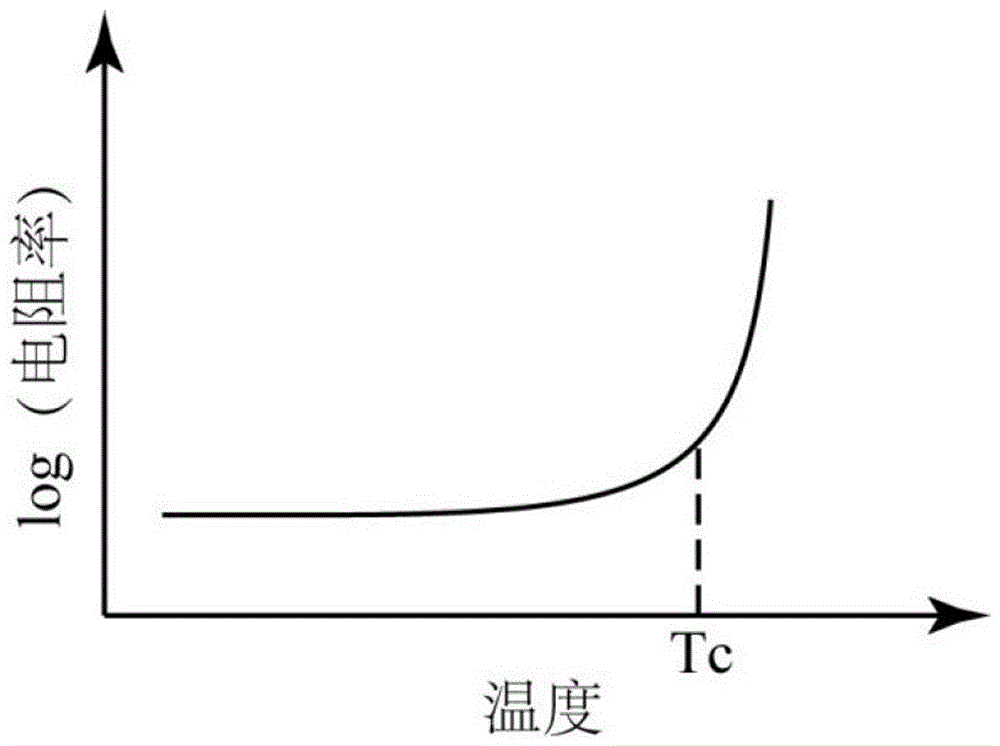
[0047] Use epoxy resin as the polymer matrix material, indium tin oxide (ITO) as the conductive filler, and mix uniformly according to the volume ratio of 1:0.4 to make the conductive polymer composite material. The conductive polymer composite material is evenly coated on the epitaxial layer by a spin coating method. Then the epitaxial wafer was placed in an oven and cured at 110° C. for 10 minutes. After standard photolithography and etching processes, a transparent conductive layer with variable resistivity is formed with a thickness of 1200A. After standard photolithography, evaporation, and alloying processes, the metal electrodes are fabricated. Finally, the substrate is ground and polished, and the epitaxial wafer is cut into an area of about 120,000 um 2 stand-alone light-emitting diode devices. The Curie temperature Tc of the variable resistivity transparent conductive layer in this embodiment is about 100° C., its resistivity at room temperature is about 50 Ωcm,...
PUM
 Abstract
Description
Claims
Application Information


