Diffusion-technology-based manufacture method for fast recovery diode chip having double buffering layers

A recovery diode and double buffer layer technology, which is used in semiconductor/solid-state device manufacturing, electrical components, circuits, etc., can solve fast recovery diode chips with large reverse recovery peak current, unfavorable manufacturing of high-voltage fast recovery diode chips, and parameter requirements. Advanced problems, to achieve the effect of shortening the width of the base area, low cost, and short recovery time

Active Publication Date: 2016-09-28
BEIJING MXTRONICS CORP +1
View PDF4 Cites 17 Cited by
  • Summary
  • Abstract
  • Description
  • Claims
  • Application Information

AI Technical Summary

Problems solved by technology

Using P+NN+ epitaxial wafers as the original silicon wafers shortens the diffusion time and simplifies the process, but its disadvantages are: (1) High-voltage fast recovery diodes have high requirements on the parameters of the epitaxial material, requiring thick epitaxy and low resistance (For example, for high-voltage fast recovery diodes, the resistivity of the P+ layer in the material is usually required to be 0.001Ω·cm, the thickness of the P+ layer is required to be about 100μm, the resistivity of the N layer material is required to be 1-200Ω·cm, and the thickness is 1-400μm). The epitaxy technology is difficult , so it is not conducive to the manufacture of high-voltage fast recovery diode chips; (2) The pn junction of the diode made of P+NN+ epitaxial material is a sudden junction, and the reverse extraction speed of the carrier is fast during the reverse recovery of the diode, which is used for recombination. Therefore, the reverse recovery peak current of the fast recovery diode chip made by this kind of processing extension structure is large, which belongs to hard recovery; (3) the current three-layer epitaxial material of domestic manufacturers cannot meet the design requirements, and the cost of using imported materials is high. The procurement cycle is long and the cost performance of chips is low

Method used


Image

  • Diffusion-technology-based manufacture method for fast recovery diode chip having double buffering layers
  • Diffusion-technology-based manufacture method for fast recovery diode chip having double buffering layers
  • Diffusion-technology-based manufacture method for fast recovery diode chip having double buffering layers

Examples


specific Embodiment approach

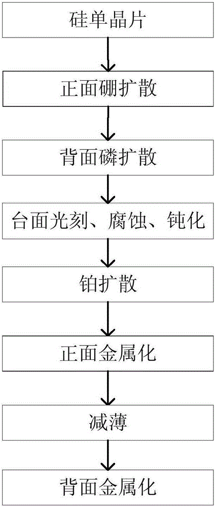
[0046] By adopting the manufacturing method of the invention, the anode and the cathode of the fast recovery diode chip are formed by diffusion, the process steps are simple, and the fast recovery diode chip with low cost, high withstand voltage, short recovery time and soft recovery characteristics can be manufactured. The specific implementation is as follows:

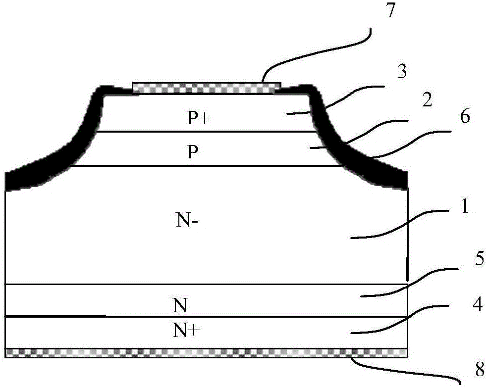
[0047] (1) Use N-type single-polished silicon single wafer as the base material, deposit oxide layer and silicon nitride layer on the non-polished surface of this N-type silicon single wafer, and then use boron-doped latex as the impurity source, at 1100 ~ Boron diffusion is performed on the polished surface of N-type silicon single wafer at 1250°C for 10-20 hours, and a diode anode is formed on the polished surface of N-type silicon single wafer, even if the N-type silicon single wafer forms an N-type silicon single wafer with a diode anode. wafer. The anode structure formed by diffusion is a P+P structure. The exi...


PUM


Abstract

The invention relates to a diffusion-technology-based manufacture method for a fast recovery diode chip having a double-buffer-layer structure. During a manufacture process, reverse recovery charges and reverse recovery time are reduced and effect of reverse recovery peak current is inhibited. The fast recovery diode is formed by adopting a phosphorus deep diffusion mode and a cathode structure formed by the diffusion is an N+N structure, an N area is a buffering layer which can block expansion of a space charge area, shortens a width of a base area and reduces forward on-state voltage drop; when the diode is reverse, an electric field between an N-N interface and an NN+ interface slows down carrier reverse drawing speed, which enables more charges to be used for recombination and softens the recovery characteristics. The diffusion-technology-based manufacture method adopts the diffusion mode to form the anode and the cathode of the fast recovery diode chip, combines with the platinum diffusion minority carrier life control technology, has a simple manufacture technology process and can manufacture the fast recovery diode chip which is low in cost, high in voltage resistance, short in recovery time and has soft recovery characteristics.

Description

technical field [0001] The invention relates to a method for manufacturing a fast recovery diode chip with a double buffer layer based on a diffusion process, that is, a method for manufacturing a fast recovery diode chip with a double buffer layer based on a diffusion process, belonging to the field of power semiconductor devices. Background technique [0002] Fast recovery diodes are widely used in pulse width modulators, switching power supplies, uninterruptible power supplies, etc. In the device, it is used for high-frequency, high-voltage, high-current rectification, freewheeling and protection, and has become an indispensable part of the application device. [0003] The main requirements of modern electronic application devices for the performance of fast recovery diodes are: the reverse recovery time should be short to reduce the diode switching loss and increase the circuit operating frequency; the reverse recovery softness should be large to reduce the reverse recov...

Claims


Application Information

Patent Timeline
Patent Type & Authority Applications(China)
IPC IPC(8): H01L21/329H01L29/861
CPCH01L29/6609H01L29/8613
Inventor 赵元富姚全斌殷丽王传敏刘学明
Owner BEIJING MXTRONICS CORP
Why Eureka
Try Eureka