Back contact solar cell and solar cell component

A solar cell and back contact technology, applied in the field of solar cells, can solve the problems of cost increase, incompatibility, breakdown, etc., and achieve the effect of simple structure, good reverse leakage current, and good insulation effect

Active Publication Date: 2016-10-26
JA SOLAR TECH YANGZHOU
View PDF6 Cites 8 Cited by
  • Summary
  • Abstract
  • Description
  • Claims
  • Application Information

AI Technical Summary

Problems solved by technology

In the previous manufacturing process of back-contact solar cells, most of the metallization process is realized by electroplating with a relatively complicated process. Complex, the discharged waste seriously pollutes the environment, and is incompatible with the mainstream metallization method of industrial production, so it is difficult to promote low-cost industrialization
The metallization of the back contact battery using the current mainstream screen printing technology. If the conventional busbar design is adopted, the two main problems faced are 1. Between the busbar and the opposite electrode thin grid and between the busbar and the opposite electrode. Insulation between doped regions corresponding to electrodes
2. In order to reduce the line resistance on the main grid line and the thin grid line, wider grid lines are required, and more paste consumption will lead to a sharp increase in cost
Due to the printing method and the characteristics of the insulating paste that limit the thickness of the paste and the tip effect caused by the uneven surface of the silicon wafer, the insulation effect is not ideal, and breakdown will occur in a local area, resulting in reverse leakage current of the cell. increase

Method used


Image

  • Back contact solar cell and solar cell component
  • Back contact solar cell and solar cell component
  • Back contact solar cell and solar cell component

Examples


Embodiment 1

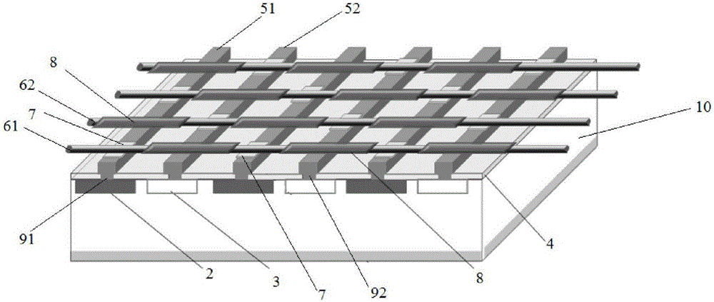
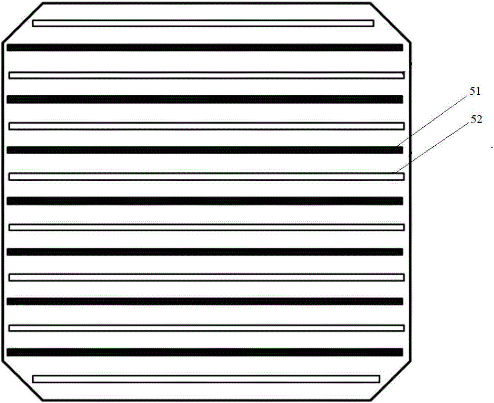
[0053] Such as figure 1 and image 3 As shown, a back-contact solar cell provided in this embodiment includes an n-type silicon substrate 10, a p+ doped region 2, an n+ doped region 3, a passivation antireflection layer 4, a positive electrode fine grid 51 and a negative electrode fine grid. The gate 52, the p+ doped region 2 and the n+ doped region 3 are alternately arranged and distributed on the back of the n-type silicon substrate 10, the passivation antireflection layer 4 is arranged on the p+ doped region 2 and the n+ doped region 3, and the positive electrode The fine grid 51 is arranged on the passivation anti-reflection layer 4 and connected to the p+ doped region 2, the negative electrode fine grid 52 is arranged on the passivation anti-reflection layer 4 and connected to the n+ doped region 3, and also includes a positive electrode The conductive wire 61 and the negative electrode conductive wire 62, the positive electrode conductive wire 61 is arranged on the posi...

Embodiment 2

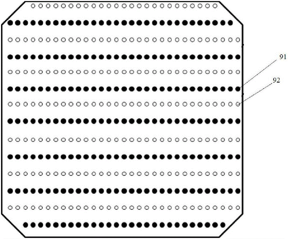
[0084] Such as figure 1 and image 3 As shown in , the back contact solar cell provided by this embodiment includes an n-type monocrystalline silicon substrate, an n+ front field and a front passivation layer arranged on the front side of the silicon substrate, a p+ doped region 2 and a front passivation layer arranged on the back side of the silicon substrate N+ doped regions 3, p+ doped regions 2 and n+ doped regions 3 are alternately arranged on the back of the silicon substrate, the passivation antireflection layer 4 is used for passivation of the back surface, and a positive electrode is provided on the p+ doped regions 2 A contact point 91, a negative electrode contact point 92 is provided on the n+ doped region 3, and a positive electrode fine grid 51 and a negative electrode fine grid 52 are also provided on the back side of the silicon substrate, respectively connecting the positive electrode contact point 91 and the negative electrode contact point 92.

[0085] Amo...

Embodiment 3

[0097] Different from Example 1, the preparation method of the back contact solar cell module is as follows:

[0098] (1) Select an n-type crystalline silicon wafer, and make p+ doped regions and n+ doped regions alternately arranged and distributed on the back side of the n-type crystalline silicon wafer;

[0099] (2) A passivation antireflection layer is provided on the p+ doped region and n+ doped region, a positive electrode contact point and a negative electrode contact point are arranged on the passivation antireflection layer, and a positive electrode fine grid is arranged on the positive electrode contact point Connecting them, setting the negative electrode fine grid on the negative electrode contact point and connecting them;

[0100] (3) The positive electrode conductive wire and the negative electrode conductive wire are arranged on the positive electrode contact fine grid and the negative electrode contact fine grid, wherein the positive electrode conductive wire ...


PUM


Abstract

The invention discloses a back contact solar cell, including an n type silicon substrate, a P + doped region, an N + doped region, a passivation and anti-reflection layer, a positive electrode fine grid and a negative electrode fine grid as well as a positive electrode wire and a negative electrode wire. The positive electrode wire is arranged in the positive electrode fine grid the negative electrode fine grid. The contact part between the positive electrode wire and positive electrode fine grid is provided with a conductive material. The positive electrode wire at the contact part between the positive electrode wire and the negative electrode fine grid is wrapped with an insulating material. The negative electrode wire is arranged in the positive electrode fine grid and negative electrode fine grid. The contact part between the negative electrode wire and negative electrode fine grid is provided with a conductive material. The negative electrode wire at the contact part between the negative electrode wire and the positive electrode fine grid is wrapped with an insulating material. The back contact solar cell can reduce the influence of the fine grid on resistance, reduce the use amount of silver paste, increase the filling factor, and reduce the shielding effect of the back metal on the back of the incident light.

Description

technical field [0001] The invention belongs to the field of solar cells, and in particular relates to a back-contact solar cell and a solar cell assembly. Background technique [0002] A solar cell is a semiconductor device that converts light energy into electrical energy. Lower production costs and higher energy conversion efficiency have always been the goals pursued by the solar cell industry. For conventional solar cells at present, the positive electrode contact electrode and the negative electrode contact electrode are respectively located on the front and back sides of the battery sheet. The front of the battery is the light-receiving surface, and the coverage of the metal positive electrode on the front will inevitably cause a part of the incident sunlight to be reflected by the metal electrode, resulting in a part of optical loss. The coverage area of ​​the front metal electrode of an ordinary crystalline silicon solar cell is about 7%, and reducing the front cov...

Claims


Application Information

Patent Timeline
Patent Type & Authority Applications(China)
IPC IPC(8): H01L31/0224H01L31/05
CPCH01L31/022441H01L31/0516Y02E10/50
Inventor 蒋秀林孙寿亮黄卓周艳方单伟
Owner JA SOLAR TECH YANGZHOU
Why Eureka
Try Eureka