Microstructure silicon-based material, preparation method thereof and semiconductor device

A technology of silicon-based materials and manufacturing methods, applied in semiconductor devices, microstructure technology, electric solid-state devices, etc., can solve the problems of cumbersome processing steps and high processing costs of imaging sensors, and achieve low cost, simple manufacturing methods, and simple processes Effect

Inactive Publication Date: 2016-11-09
CHANGCHUN INST OF OPTICS FINE MECHANICS & PHYSICS CHINESE ACAD OF SCI
View PDF6 Cites 6 Cited by
  • Summary
  • Abstract
  • Description
  • Claims
  • Application Information

AI Technical Summary

Problems solved by technology

[0006] In view of this, the present invention provides a microstructured silicon-based material, a manufacturing method thereof, and a semiconductor

Method used


Image

  • Microstructure silicon-based material, preparation method thereof and semiconductor device
  • Microstructure silicon-based material, preparation method thereof and semiconductor device
  • Microstructure silicon-based material, preparation method thereof and semiconductor device

Examples


Embodiment Construction

[0053] The following will clearly and completely describe the technical solutions in the embodiments of the present invention with reference to the accompanying drawings in the embodiments of the present invention. Obviously, the described embodiments are only some, not all, embodiments of the present invention. Based on the embodiments of the present invention, all other embodiments obtained by persons of ordinary skill in the art without making creative efforts belong to the protection scope of the present invention.

[0054] The invention provides a method for making a microstructured silicon-based material, such as figure 1 shown, including:

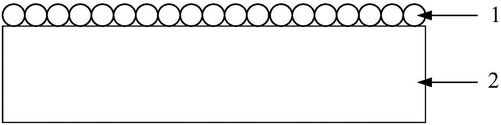
[0055] Step S101: providing silicon wafer and microsphere solution.

[0056] It should be noted that the doping type of the silicon wafer is not limited in the present invention, nor is the crystal orientation of the silicon wafer. Preferably, the silicon wafer in this embodiment is n-type and crystallographic to 100 wafers. Those...


PUM


Abstract

The invention provides a microstructure silicon-based material, a preparation method thereof and a semiconductor device. The preparation method comprises the steps of providing a silicon wafer and microsphere solution; prepraring the microsphere solution into a microsphere template by employing a self-assembly mode; transferring the self-assembly template to the surface of the silicon wafer, and carrying out annealing heat treatment; and etching the silicon wafer by taking microspheres as masks and employing a reaction ion beam etching technology, washing the silicon wafer, and coating film, thereby forming a metal nanocone-shaped microstructure. According to the preparation method provided by the invention, firstly, the microsphere template obtained by employing the self-assembly mode is taken as the mask, and compared with the mask prepared by a special mask preparation technology in the prior art, the mask provided by the invention has the advantages of simple in preparation method and relatively low in cost; and secondly, according to the preparation method provided by the invention, the silicon wafer is etched by employing the relatively cheap reaction ion beam etching technology, and compared with the micro-nano machining methods such as a focusing ion beam etching technology, electron beam lithography and laser direct writing in the prior art, the preparation method has the advantages of simple technology and relatively low cost.

Description

technical field [0001] The invention relates to the technical field of semiconductor optoelectronic materials, in particular to a microstructured silicon-based material, a manufacturing method thereof, and a semiconductor device. Background technique [0002] At present, according to the types of chip materials, imaging sensors can be roughly divided into visible light imaging sensors based on silicon-based materials and infrared light imaging sensors based on non-silicon-based materials. Silicon-based imaging sensors have the advantages of mature manufacturing process, low cost, simple device structure, can work at room temperature, and strong environmental resistance. At present, silicon-based imaging sensors have been widely used in people's daily life, such as mobile phone cameras, SLR The core imaging elements of the camera are all made of silicon-based CMOS imaging sensors, but the photosensitive area of ​​silicon-based imaging sensors is mainly concentrated in the vis...

Claims


Application Information

Patent Timeline
IPC IPC(8): B81C1/00H01L27/146
CPCB81C1/00B81C1/00015H01L27/146H01L27/14683
Inventor 杨海贵李强高劲松刘小翼王延超李资政王笑夷
Owner CHANGCHUN INST OF OPTICS FINE MECHANICS & PHYSICS CHINESE ACAD OF SCI
Why Eureka
Try Eureka