Method for preparing metal oxide thin-film resistive random access memory through plasma processing

A technology of oxide thin film and resistive memory, which is applied in semiconductor/solid-state device manufacturing, electrical components, circuits, etc., can solve the problems affecting the stability of device performance, long response time, low efficiency, etc., and achieve good consistency and integration High density and good consistency

Active Publication Date: 2016-11-09
UNIV OF ELECTRONICS SCI & TECH OF CHINA
View PDF4 Cites 11 Cited by
  • Summary
  • Abstract
  • Description
  • Claims
  • Application Information

AI Technical Summary

Problems solved by technology

However, at present, more oxygen plasma treatment is used, which is not easy to completely oxidize titanium to +4 valence, which affects the stability of device performance.
At the same time, the efficiency of defect introduction is not high, requiring higher voltage and longer reaction time

Method used


Image

  • Method for preparing metal oxide thin-film resistive random access memory through plasma processing
  • Method for preparing metal oxide thin-film resistive random access memory through plasma processing
  • Method for preparing metal oxide thin-film resistive random access memory through plasma processing

Examples


Embodiment Construction

[0030] Concrete implementation steps of the present invention:

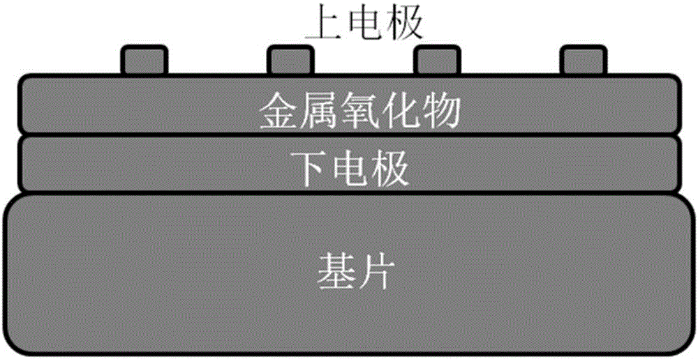
[0031] Step 1: Prepare a metal thin film electrode on a silicon substrate. The substrate is a commercially purchased silicon substrate with a P-doped 110 crystal plane.

[0032] Step 2: Deposit the lower electrode metal film. Platinum was chosen as the metal of the lower electrode in the experiment, and it was prepared directly on the silicon substrate by magnetron sputtering. After the sample is placed in the sputtering chamber, the vacuum is evacuated to a pressure of 6×10⁻⁴Pa. Argon gas is then introduced and a DC voltage is applied between the chamber and the target. The target is a disk-shaped metal block made of metal platinum. When the voltage reaches 420 volts, a certain concentration of argon plasma is generated. Under this condition, the sputtering rate of platinum is about 12 nanometers per minute, and the sputtering time is 8 minutes, so the thickness of the obtained metallic platinum is about 20...


PUM

PropertyMeasurementUnit
thicknessaaaaaaaaaa
thicknessaaaaaaaaaa
thicknessaaaaaaaaaa

Abstract

The invention provides a method for preparing a metal oxide thin-film resistive random access memory through plasma processing, wherein the method belongs to the technical field of electronic films and components. The memory comprises the components of a substrate, a lower electrode, a fluorine-doped metal oxide and an upper electrode. According to the method, a relatively novel plasma processing method is utilized for conveniently and controllably preparing a metal oxide resistive random access functional layer with uniform defect distribution. The metal oxide resistive random access functional layer can conveniently and quickly realize switching between formation and switching-off of a conductive channel under the function of an electric field, namely switching between a low-resistance state and a high-resistance state of the device. Furthermore, the method has an ultralow working voltage. The upper electrode is prepared through a mask method, thereby greatly reducing device dimension and improving integration density. Through testing, the metal oxide thin-film resistive random access memory prepared according to the method has excellent performance. In one word, the invention realizes the method for preparing the metal oxide thin-film resistive random access memory with advantages high performance and small dimension, wherein the method has advantages of simple operation, effective controllability, high efficiency and low cost. Furthermore relatively high performance consistency is realized. The method is suitable for batch resistive random access array production in future, and furthermore has good application prospect.

Description

technical field [0001] The invention belongs to the technical field of electronic thin films and components, in particular to a conductive filament type resistive variable memory based on a silicon-based substrate. Background technique [0002] Resistive random access memory (RRAM) is a non-volatile memory device (NVM) that controls data storage and reading based on resistance changes. This type of memory is considered to be one of the important research directions for future memory development because of its low power consumption, high storage density, high read / write rate, simple structure, and easy miniaturization. The resistive switch layer of this type of memory device is generally dominated by binary and ternary oxide films. Including titanium oxide, nickel oxide, zirconium oxide, aluminum oxide, oxide, lithium niobate, bismuth ferrite, etc. As one of the traditional N-type binary oxides, titanium oxide has the characteristics of controllable structure, easy preparat...

Claims


Application Information

Patent Timeline
Patent Type & Authority Applications(China)
IPC IPC(8): H01L45/00H01L21/3065
CPCH01L21/3065H10N70/8833H10N70/011
Inventor 吴传贵孙翔宇帅垚潘忻强白晓园张万里
Owner UNIV OF ELECTRONICS SCI & TECH OF CHINA
Why Eureka
Try Eureka