A kind of perovskite thin film phototransistor and preparation method thereof

A phototransistor, perovskite technology, applied in the field of photodetectors, to achieve the effect of increasing quantum efficiency, strong visible light absorption characteristics, and high device success rate

Active Publication Date: 2018-06-15
PEKING UNIV SHENZHEN GRADUATE SCHOOL
View PDF5 Cites 0 Cited by
  • Summary
  • Abstract
  • Description
  • Claims
  • Application Information

AI Technical Summary

Problems solved by technology

Since most metal oxide transistors are photosensitive, this advantage can be used to design phototransistors that modulate electrical signals with light (Ahn S E, Song I, Jeon S, et al. Metal oxide thin film phototransistor for remote touch interactive displays[J ].Advanced Materials, 24, 19, 2631-2636, 2012.), but IGZO has a large band gap (> 3eV), so this type of oxide has almost no response to the visible light band with a wavelength greater than 420nm

Method used


Image

  • A kind of perovskite thin film phototransistor and preparation method thereof
  • A kind of perovskite thin film phototransistor and preparation method thereof
  • A kind of perovskite thin film phototransistor and preparation method thereof

Examples


preparation example Construction

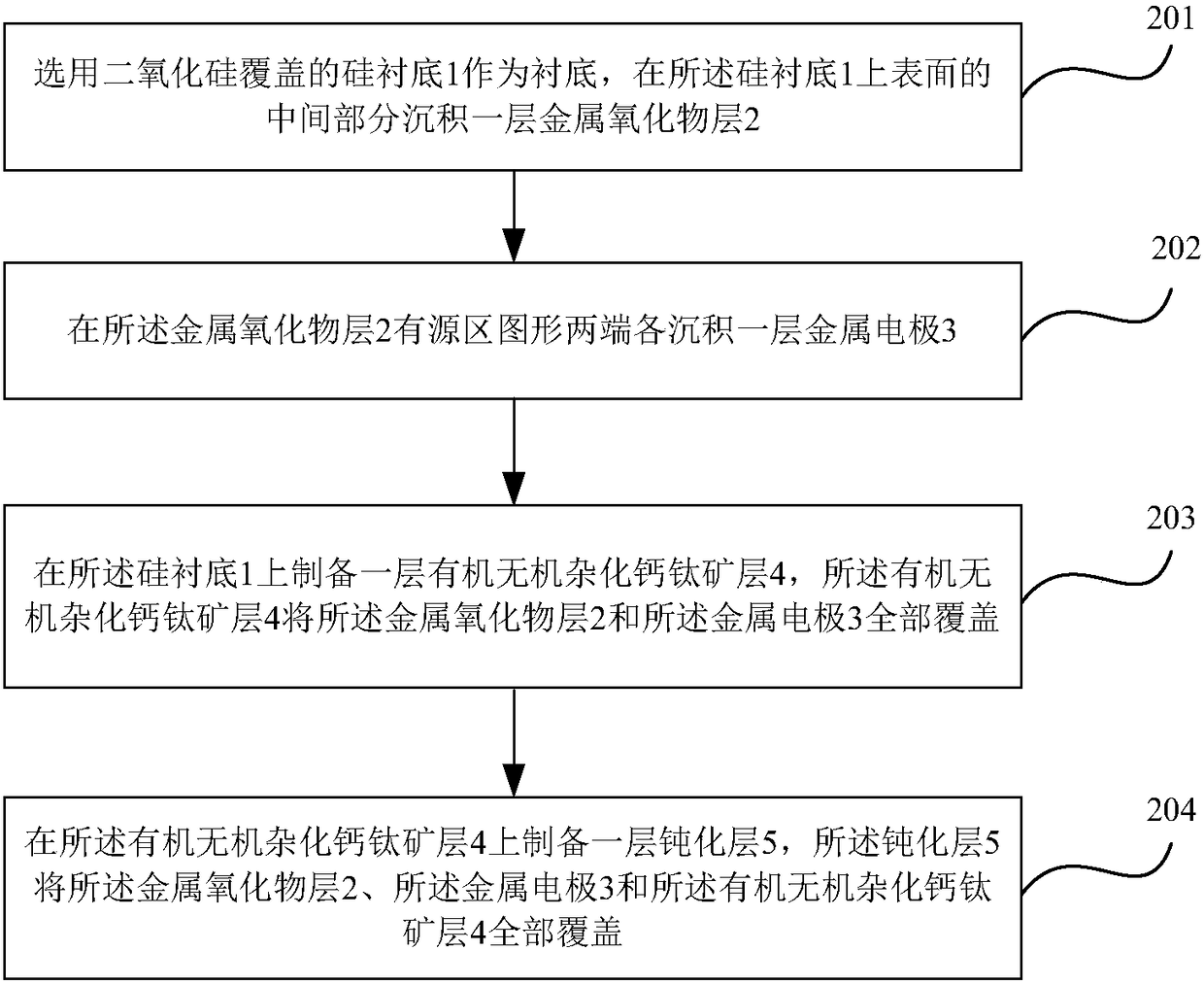
[0025] Corresponding to the above method embodiment, such as figure 2 As shown, it is a kind of embodiment of the present invention figure 1 The flow chart of the preparation method of the perovskite thin film phototransistor shown, the method comprises:

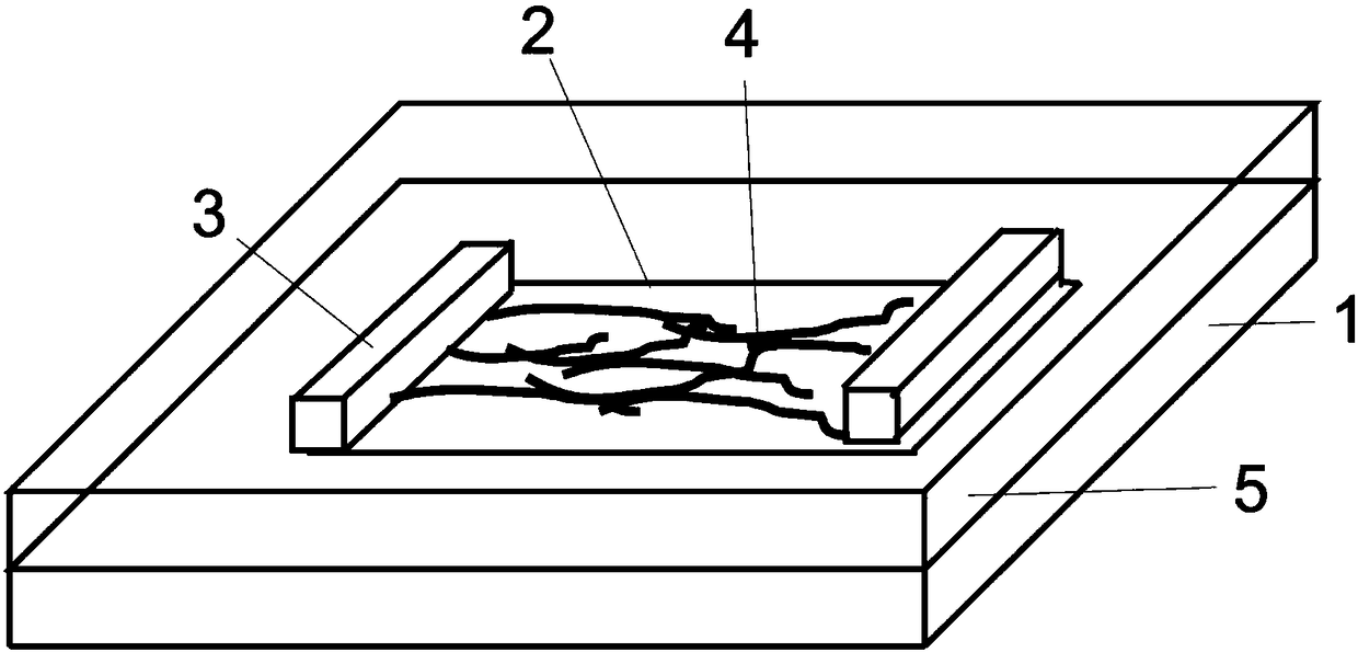
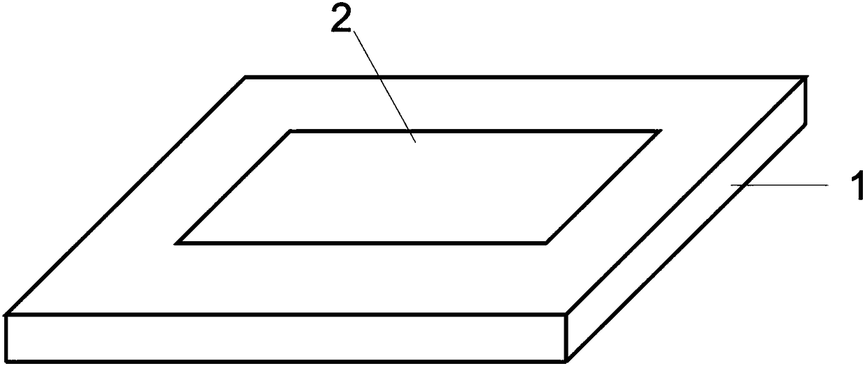
[0026] 201. Select a silicon substrate 1 covered with silicon dioxide as the substrate, and deposit a layer of metal oxide layer 2 on the middle part of the upper surface of the silicon substrate 1; image 3 It is a schematic structural view of a silicon substrate covered with silicon oxide covered with a metal oxide layer according to an embodiment of the present invention;

[0027] 202. Deposit a layer of metal electrodes 3 on both ends of the pattern in the active area of ​​the metal oxide layer 2; Figure 4 It is a schematic diagram of the structure after the metal oxide layer is plated with metal electrodes according to the embodiment of the present invention;

[0028] 203. Prepare a layer of organic-inorganic hybri...


PUM

PropertyMeasurementUnit
thicknessaaaaaaaaaa
thicknessaaaaaaaaaa
thicknessaaaaaaaaaa

Abstract

An embodiment of the present invention provides a perovskite thin film phototransistor and a preparation method thereof. The perovskite thin film phototransistor includes: a silicon substrate covered with silicon dioxide, and the middle part of the upper surface of the silicon substrate is covered with A metal oxide layer, the two ends of the metal oxide layer are plated with source and drain metal electrodes, the middle is an organic-inorganic hybrid perovskite layer, and a passivation layer is arranged above the silicon substrate. The oxide layer completely covers the metal oxide layer and the organic-inorganic hybrid perovskite material layer. The invention can combine the metal oxide semiconductor with the organic-inorganic hybrid perovskite, has simple preparation process, high device success rate, and has great potential for fast response and wide-spectrum light detection.

Description

technical field [0001] The invention relates to the field of photodetectors, in particular to a perovskite thin film phototransistor and a preparation method thereof. Background technique [0002] Amorphous metal oxides represented by zinc tin oxide, indium gallium zinc oxide (IGZO) and indium zinc oxide have attracted the attention of a large number of researchers due to their excellent performance and wide application. Since most metal oxide transistors are photosensitive, this advantage can be used to design phototransistors that modulate electrical signals with light (Ahn S E, Song I, Jeon S, et al. Metal oxide thin film phototransistor for remote touch interactive displays[J ]. Advanced Materials, 24, 19, 2631-2636, 2012.), but IGZO has a large forbidden band width (> 3eV), so this type of oxide has almost no response to the visible light band with a wavelength greater than 420nm. This shortcoming can be overcome by combining a narrow bandgap photosensitive semicond...

Claims


Application Information

Patent Timeline
Patent Type & Authority Patents(China)
IPC IPC(8): H01L51/42H01L51/46H01L51/48
CPCH10K85/30H10K30/65H10K2102/00Y02E10/549Y02P70/50
Inventor 周航杜嵩楠王琰
Owner PEKING UNIV SHENZHEN GRADUATE SCHOOL
Why Eureka
Try Eureka