A kind of crystalline silicon solar cell and its preparation method

A technology of solar cells and crystalline silicon, which is applied in circuits, electrical components, photovoltaic power generation, etc., can solve the problems of increased battery series resistance, decreased fill factor, and damaged passivation layer, and achieves increased open circuit voltage, Isc, and The effect of increasing the light path

Active Publication Date: 2018-03-27
BYD CO LTD
View PDF7 Cites 0 Cited by
  • Summary
  • Abstract
  • Description
  • Claims
  • Application Information

AI Technical Summary

Problems solved by technology

[0004] After depositing aluminum oxide and silicon nitride layers on the backlight surface of the silicon wafer, because the aluminum oxide and silicon nitride layers are poor conductors of electricity, even if the method of laser grooving is used to make the aluminum paste sinter and contact the silicon on the back surface to form a photo-generated carrier. However, due to the small area of ​​laser grooves and the poor lateral transport performance of photogenerated carriers, the series resistance of the battery increases and the fill factor decreases
On the other hand, after the aluminum oxide passivation layer is prepared, it is necessary to anneal the deposited passivation layer at a higher temperature to improve the effect of the passivation layer. In this process, the long-term high-temperature annealing process may cause Increased defect density in silicon wafers
In addition, the aluminum paste is printed on the entire area of ​​the silicon nitride protective layer. After sintering, the glass powder in the aluminum paste may corrode and penetrate the silicon nitride and The aluminum oxide layer causes the aluminum paste to damage the passivation layer, thereby weakening the effect of the passivation layer on improving the photoelectric performance of the battery to a certain extent

Method used


Image

  • A kind of crystalline silicon solar cell and its preparation method
  • A kind of crystalline silicon solar cell and its preparation method
  • A kind of crystalline silicon solar cell and its preparation method

Examples


preparation example Construction

[0037] The present invention also provides a method for preparing the above-mentioned crystalline silicon solar cell, which specifically includes the following steps:

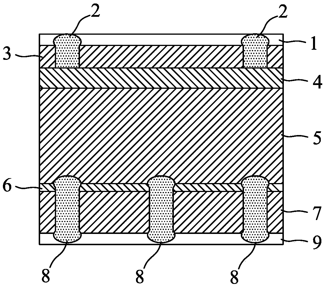
[0038] S1. Provide a silicon substrate with a diffusion layer on the light-facing surface, the silicon substrate is a P-type polycrystalline silicon-silicon substrate, and a P-type zinc oxide is deposited on the backlight surface of the silicon substrate to form a conductive medium layer;

[0039] S2. Prepare a protective layer on the conductive medium layer, and then prepare an aluminum back field on the protective layer, the aluminum back field penetrates the conductive medium layer and the protective layer, and is in contact with the silicon substrate and the conductive medium layer at the same time;

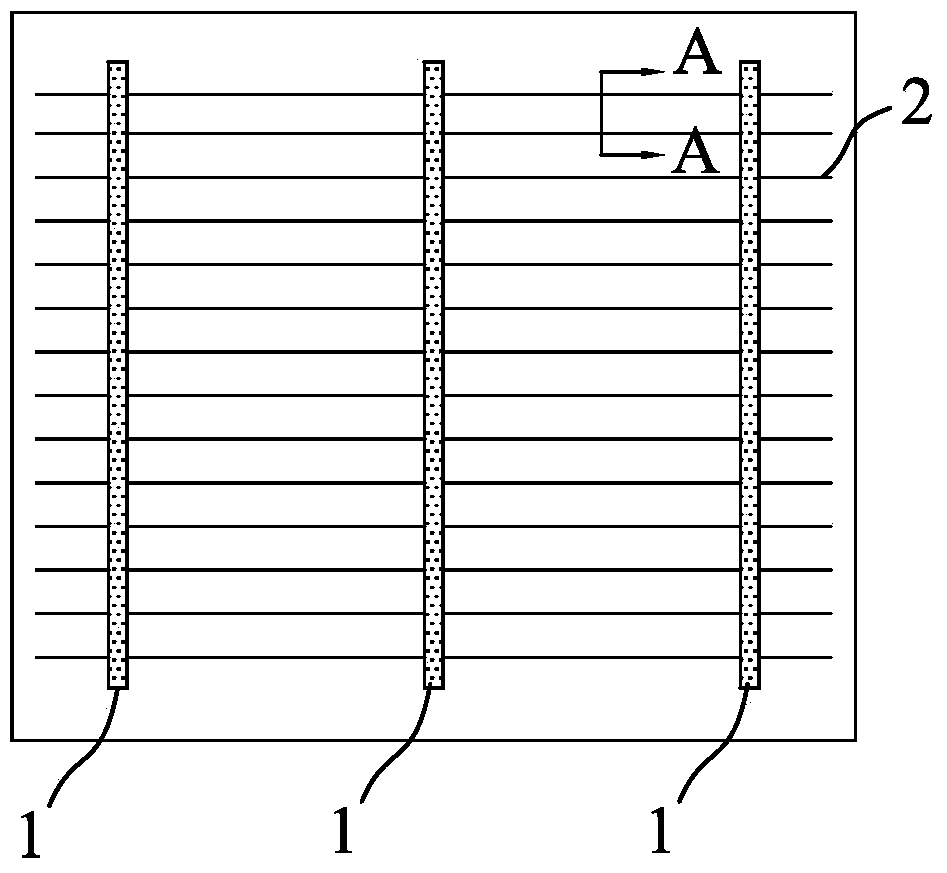
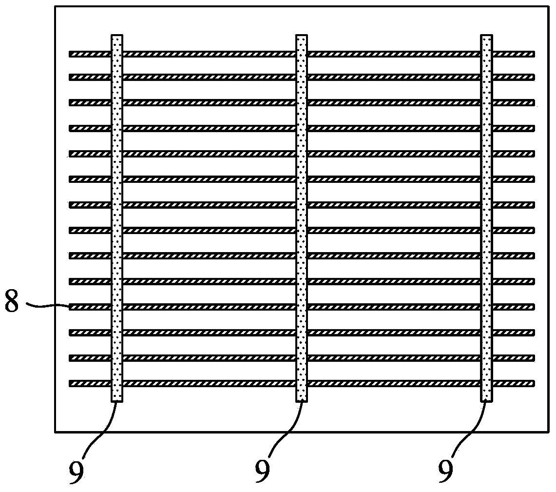
[0040] S3. On the protective layer on the backlight surface of the silicon substrate, prepare electrode grid lines on the backlight surface that are in contact with the aluminum back field, and prepare electrode ...

Embodiment 1

[0069] This embodiment is used to illustrate the crystalline silicon solar cell and its preparation method disclosed in the present invention.

[0070] 1. Preparation of silicon wafers before coating

[0071] The specification of the P-type polycrystalline silicon wafer used is: 156mm×156mm, and the thickness is 200μm. After the silicon wafer is textured, diffused and etched, the back of the silicon wafer is polished to obtain a silicon substrate with a diffusion layer on the surface.

[0072] 2. Preparation of P-type zinc oxide conductive dielectric layer

[0073] Solay Tech InPassion ALD 3600 atomic layer deposition equipment produced in the Netherlands was adopted, and dimethyl zinc, ammonia gas, trimethyl aluminum and deionized water were used as the zinc source, nitrogen source, aluminum source and oxygen source required for deposition, and dimethyl The molar ratio of base zinc: ammonia: trimethylaluminum: deionized water is 1:2:0.05:4. The temperature of the silicon su...

Embodiment 2

[0087] This embodiment is used to illustrate the crystalline silicon solar cell and its preparation method disclosed in the present invention.

[0088] Change the deposition time of the P-type zinc oxide conductive medium layer in embodiment 1 step 2 to 60 seconds, and the deposition thickness is 90-95nm. The resistivity of the conductive medium layer is tested to be 0.0453Ωcm. All the other processes and other steps are carried out Example 1 is the same.

[0089] The obtained crystalline silicon solar cell is denoted as S2.


PUM

PropertyMeasurementUnit
thicknessaaaaaaaaaa
widthaaaaaaaaaa
thicknessaaaaaaaaaa

Abstract

In order to improve photoelectric conversion efficiency of a crystalline silicon solar cell, the invention provides a novel crystalline silicon solar cell includes a silicon substrate. The backlight face of the silicon substrate is provided with a conducting dielectric layer, a protection layer and a backlight face electrode grid line in sequence. The conducting dielectric layer is in contact with the silicon substrate. An aluminum back surface field is also arranged between the silicon substrate and the backlight face electrode grid line. The aluminum back surface field penetrates through the conducting dielectric layer and the protection layer and is in contact with the silicon substrate, the conducting dielectric layer and the backlight face electrode grid line. The conducting dielectric layer is made of P type zinc oxide. At the same time, the invention also discloses a preparation method of the above crystalline silicon solar cell. The photoelectric conversion efficiency of the crystalline silicon solar cell provided by the invention is high.

Description

technical field [0001] The invention relates to a crystalline silicon solar cell and a preparation method thereof. Background technique [0002] With the development of the solar industry and the intensification of competition, customers have higher and higher requirements for the efficiency of solar cells, and the entry threshold of the industry is also increasing. Therefore, it is necessary to explore more industrialization technologies to improve the conversion efficiency of solar cells. At present, the technology of solar cells to the light side is very mature, and the focus of improving the conversion efficiency is gradually shifting to the back side with great potential. With the help of atomic layer deposition (ALD) technology, the rear passivation battery with aluminum oxide passivation layer deposited on the back has become a bright spot at present. Passivated emitter and rear surface passivated cell (PERC) is mainly based on the good passivation effect of aluminum...

Claims


Application Information

Patent Timeline
Patent Type & Authority Patents(China)
IPC IPC(8): H01L31/068H01L31/0224H01L31/0216H01L31/18
CPCY02E10/547Y02P70/50
Inventor 谭伟华左静鹿兆岩
Owner BYD CO LTD
Why Eureka
Try Eureka