

MEMS device, method for manufacturing MEMS device, and electronic device
A technology for electronic devices and devices, applied in the field of MEMS devices and their preparation, can solve problems such as device damage, and achieve the effects of suppressing damage, protecting devices, and improving yield
- Summary
- Abstract
- Description
- Claims
- Application Information
AI Technical Summary
Problems solved by technology
Method used
Image

Examples
preparation example Construction
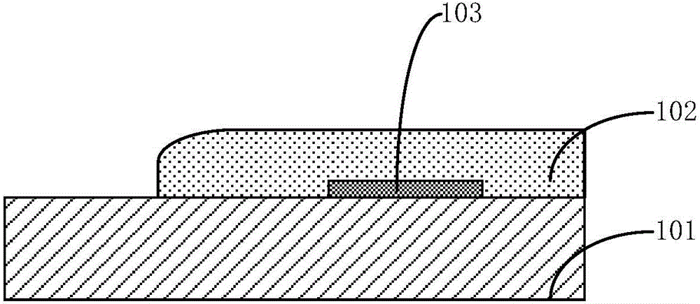
[0040] At present, the preparation methods of MEMS devices are as follows: Figures 1a-1e As shown, the method will be further described below in conjunction with the accompanying drawings. First, a semiconductor substrate 101 is provided, and a MEMS device 103 is formed on the semiconductor substrate 101, such as a vibrating membrane or a sensing membrane, etc., to obtain the following: Figure 1a pattern shown.
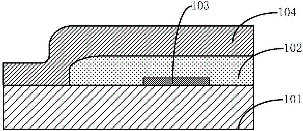
[0041] Next, a sacrificial material layer 102 is formed on the semiconductor substrate and patterned to expose part of the semiconductor substrate to form a stepped pattern, so as to obtain Figure 1b pattern shown.
[0042] depositing a functional material layer 104 to cover the semiconductor substrate and the sacrificial material layer 102, so as to obtain Figure 1b pattern shown.
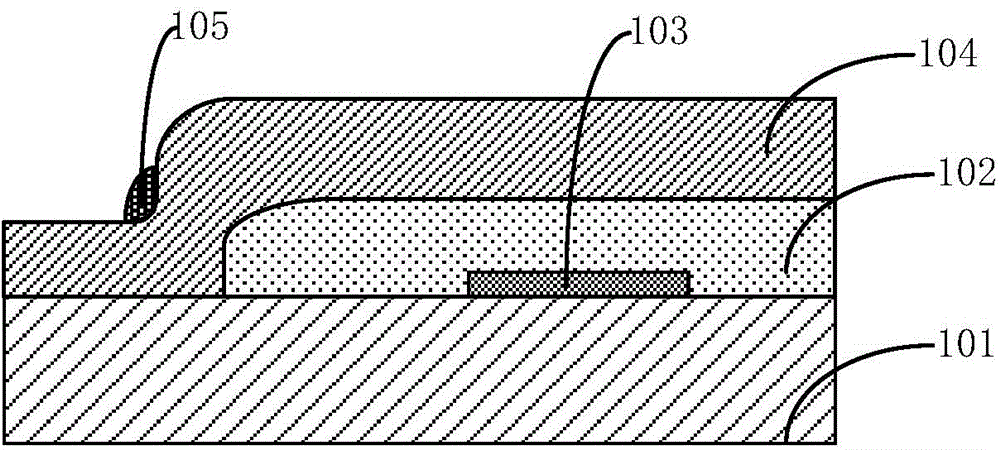
[0043] A spacer wall 105 is formed on the sidewall of the functional material layer 104, so as to obtain Figure 1c pattern shown.
[0044] A metal layer 106 is formed on the side...
Embodiment 1
[0049] The present invention also provides a kind of preparation method of described MEMS device, below in conjunction with Figures 2a-2g To further illustrate the method, 2a-2g are schematic diagrams of the fabrication process of the MEMS device in this embodiment.
[0050] First, step 201 is performed to provide a semiconductor substrate 201 on which a sacrificial layer 202 partially covering the semiconductor substrate 201 is formed to form a stepped structure.
[0051] Specifically, such as Figure 2a As shown, in this step, the semiconductor substrate 201 may be at least one of the materials mentioned below: silicon, silicon-on-insulator (SOI), silicon-on-insulator (SSOI), and germanium-on-insulator Silicon (S-SiGeOI), silicon germanium on insulator (SiGeOI) and germanium on insulator (GeOI), etc.
[0052] A MEMS element 203 is formed on the semiconductor substrate 201, wherein the MEMS element 203 can be selected according to the type of MEMS device, for example, it c...
Embodiment 2
[0084] The present invention also provides a MEMS device, which is prepared by the method described in Example 1. The semiconductor device prepared by the method described in Embodiment 1 of the present invention can improve the film composite layer, so that the metal at the corner of the device has no cracks, and can lower the corrosion of wet chemical etchant (Wet Chemical), protect the device, and further improve The performance and yield of the MEMS device are improved.
PUM
| Property | Measurement | Unit |
|---|---|---|
| Thickness | aaaaa | aaaaa |
Abstract
Description
Claims
Application Information