Method for patterning colossal magnetoresistance manganese oxide thin film on nanoscale

A manganese oxide, nano-scale technology, applied in the direction of electrical components, semiconductor/solid-state device manufacturing, circuits, etc., can solve the problems of removing residual glue, denaturation, and inability to achieve the effect of reducing thickness requirements and improving resolution

Active Publication Date: 2016-12-21
FUDAN UNIV
View PDF3 Cites 5 Cited by
  • Summary
  • Abstract
  • Description
  • Claims
  • Application Information

AI Technical Summary

Problems solved by technology

First of all, the width of the giant magnetoresistive manganese oxide nanowires is expected to be reduced as much as possible, reaching the order of one hundred nanometers or even tens of nanometers, which has high requirements for the type and thickness of the glue used in electron beam lithography; Secondly, if the first requirement is met, if the electron beam glue pattern is used as the etching mask layer, during argon etching, due to the similar etching rate of the huge magnetoresistive manganese oxide and the electron beam glue, it is impossible to The manganese oxide film is effectively protected, and the electron beam glue is denatured after argon etching, and the residual glue cannot be removed by existing methods; finally, the physical properties of the huge magnetoresistive manganese oxide film will change after argon etching, which is also unwanted

Method used


Image

  • Method for patterning colossal magnetoresistance manganese oxide thin film on nanoscale
  • Method for patterning colossal magnetoresistance manganese oxide thin film on nanoscale
  • Method for patterning colossal magnetoresistance manganese oxide thin film on nanoscale

Examples


Embodiment Construction

[0026] In order to make the above objects, features and advantages of the present invention more comprehensible, specific implementations of the present invention will be described in detail below in conjunction with the accompanying drawings.

[0027] In the following description, a lot of specific details are set forth in order to fully understand the present invention, but the present invention can also be implemented in other ways different from those described here, and those skilled in the art can do it without departing from the meaning of the present invention. By analogy, the present invention is therefore not limited to the specific examples disclosed below.

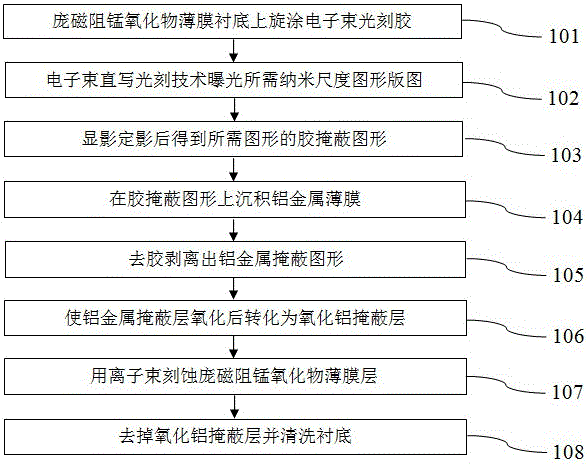
[0028] The core content of the present invention is: spin coating and baking electron beam photoresist on the strontium titanate substrate on which the huge magnetoresistive manganese oxide film has been grown; Layout; after development and fixing, the glue masking pattern of the desired nanoscale pattern is ob...


PUM


Abstract

The invention belongs to the technical field of micro-nano machining, and particularly provides a method for patterning a colossal magnetoresistance manganese oxide thin film on a nanoscale. The method comprises the steps of firstly carrying out spin-coating of electron beam photoresist on a strontium titanate substrate on which the colossal magnetoresistance manganese oxide thin film grows, carrying out baking and then exposing a required nanoscale graphic layout by use of an electron beam direct writing lithography; carrying out developing and fixing, obtaining a resist mask graphic of a required nanoscale graphic, depositing an aluminum metal thin film and then removing the resist to strip out an aluminum metal mask graphic; oxidizing an aluminum metal mask layer, transforming the aluminum metal mask layer into an aluminum oxide mask layer, and then etching the colossal magnetoresistance manganese oxide thin film by use of ion beams to form a colossal magnetoresistance manganese oxide graphic; and finally removing the aluminum oxide mask layer and cleaning the substrate. By the method, the problem that the etching rate ratio of electron beam resist to the colossal magnetoresistance manganese oxide layer during ion-beam etching is poor is solved; the thickness requirement of the electron beam resist is reduced; the resolution ratio of the electron beam direct-writing lithography is improved; and the problem that some electron beam resist cannot be easily removed after etching is also solved.

Description

technical field [0001] The invention belongs to the technical field of micro-nano processing, and in particular relates to a method for patterning a giant magnetoresistive manganese oxide film. Background technique [0002] The study of strongly correlated complex electronic systems has always been one of the cores of the research field of condensed matter physics. A strongly correlated electron system refers to a system in which the interaction between electrons cannot be ignored. In a strongly correlated system, due to the strong interaction between electrons, many novel physical phenomena are caused: such as high-temperature superconductors, multiferroics, fractional quantum Hall effect in two-dimensional magnetoresistance effect etc. Because these effects have strong application prospects in different fields, they have attracted extensive attention and stimulated great enthusiasm for research. In the strongly correlated system, due to the interaction between electron ...

Claims


Application Information

Patent Timeline
Patent Type & Authority Applications(China)
IPC IPC(8): H01L21/02H01L21/033H01L21/311
CPCH01L21/02076H01L21/0331H01L21/0332H01L21/311
Inventor 牛洁斌殷立峰沈健
Owner FUDAN UNIV
Why Eureka
Try Eureka