A Lateral Insulated Gate Bipolar Transistor with High Hot Carrier Reliability

A bipolar transistor and carrier technology, applied in semiconductor devices, electrical components, circuits, etc., can solve the problems of reduced withstand voltage and increased on-resistance of devices, and achieve reduced area and impact ionization rate. , the effect of reducing the transverse electric field

Active Publication Date: 2019-03-29
SOUTHEAST UNIV
View PDF4 Cites 0 Cited by
  • Summary
  • Abstract
  • Description
  • Claims
  • Application Information

AI Technical Summary

Problems solved by technology

Reducing the channel electric field in the on-state stage is generally achieved by reducing the doping concentration of the P-type body region, and shortening the turn-off delay is mainly achieved by increasing the doping concentration of the N-type buffer zone, but changing the P-type body region too much The doping concentration of the N-type buffer and the N-type buffer may cause a decrease in the withstand voltage of the device or an increase in the on-resistance

Method used


Image

  • A Lateral Insulated Gate Bipolar Transistor with High Hot Carrier Reliability
  • A Lateral Insulated Gate Bipolar Transistor with High Hot Carrier Reliability
  • A Lateral Insulated Gate Bipolar Transistor with High Hot Carrier Reliability

Examples


Embodiment Construction

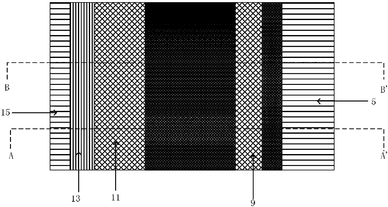
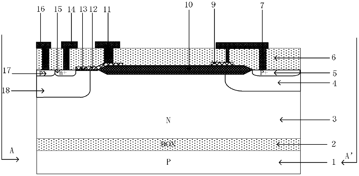
[0026] Attached below Figure 5 , the present invention is described in detail, a lateral insulated gate bipolar transistor with high hot carrier reliability, comprising: a P-type substrate 1, a buried oxide layer 2 is arranged on the P-type substrate 1, and a buried oxide layer 2 is provided with an N-type epitaxial layer 3, an N-type buffer well 4 and a P-type body region 18 are arranged inside the N-type epitaxial layer 3, and a P-type anode region 5 and an N-type floating region 18 are arranged in the N-type buffer well 4. The empty contact region 8 is provided with an N-type negative region 15 and a P-type body contact region 17 in the P-type body region 18, and a gate oxide layer 13 and a field oxide layer 10 are arranged on the surface of the N-type epitaxial layer 3, and the gate oxide layer 13 and one end of the field oxide layer 10, the other end of the gate oxide layer 13 extends to the N-type negative region 15 and ends at the boundary of the N-type negative region...


PUM


Abstract

The invention provides a transverse insulated gate bipolar transistor with high thermal carrier reliability, which comprises a P-type substrate with a buried oxide layer. An N-type epitaxial layer is provided on the buried oxide layer. In the N-type epitaxial layer, an N-type buffer well and a P-type body region are provided. In the N-type buffer well, a P-type positive region is provided. In the P-type body region, an N-type negative region and a P-type body contact region are provided. The surface of the N-type epitaxial layer is provided with a gate oxide layer and a field oxide layer. A polysilicon gate is provided on the surface of the gate oxide layer, and polysilicon is arranged on the right upper surface of the field oxide layer. The P-type positive region consists of block shaped N-type regions arranged in rows; in the N-type buffer region, a floating hollow N-type contact region is provided. The P-type positive region is arranged in the floating hollow N-type contact region, and each of the block shaped N-type regions is surrounded by the floating hollow N-type contact region on three sides. And the other end of the field oxide layer extends toward the P-type positive region and ends at the floating hollow N-type contact region. According to the invention, it is possible to reduce the emission efficiency of a parasitic PNP transistor, reduce the hot carrier damage in the on-state and the switching state, and improve the reliability of devices.

Description

technical field [0001] The present invention mainly relates to the reliability field of high-frequency and high-voltage power semiconductor devices, specifically, a lateral insulated gate bipolar transistor with high hot-carrier reliability, which is suitable for aerospace electronic equipment, satellite communication equipment, plasma display Related power integrated circuits in the fields of equipment, electronic computers, communication systems, and automobile industries. Background technique [0002] The reliability of integrated circuits has been the focus of people's attention since the birth of integrated circuits, among which Hot Carrier Injection (Hot Carrier Injection, HCI) characteristics are a very important reliability issue, and are also the main cause of failure of many electronic products. one of the reasons. With the increasing demand for energy saving, the performance of high-voltage power integrated circuit products has received more and more attention. S...

Claims


Application Information

Patent Timeline
Patent Type & Authority Patents(China)
IPC IPC(8): H01L29/739H01L29/06
CPCH01L29/0619H01L29/7393H01L29/7394
Inventor 刘斯扬方云超杨翰琪李胜叶然孙伟锋陆生礼时龙兴
Owner SOUTHEAST UNIV
Why Eureka
Try Eureka