

LED epitaxial growth method based on sapphire graphical substrate
A patterned substrate, epitaxial growth technology, applied in chemical instruments and methods, crystal growth, single crystal growth and other directions, can solve the problems of low wavelength hit rate, poor antistatic ability, low reverse voltage of epitaxial wafers, etc. The effect of crystal quality improvement, antistatic ability improvement, and reverse voltage increase
- Summary
- Abstract
- Description
- Claims
- Application Information
AI Technical Summary
Problems solved by technology
Method used
Image

Examples
Embodiment 1
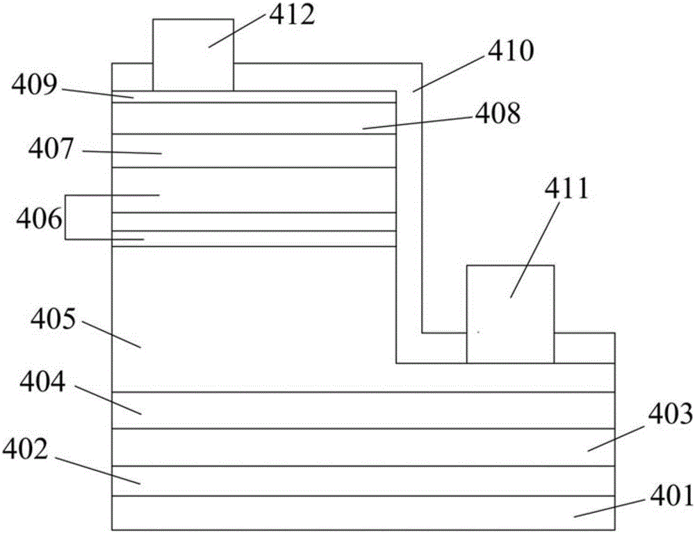
[0048] Such as figure 2 As shown, it is a schematic diagram of the LED structure based on the epitaxial growth method of the sapphire patterned substrate described in this embodiment. The method described in this embodiment solves the problem of the method for preparing LEDs in the prior art and makes the prepared epitaxial wafers have a low wavelength hit rate. , Poor crystal quality of the epitaxial wafer, poor crystal quality of the light-emitting layer, reduced doping efficiency of the P layer, and reduced hole mobility; resulting in reduced brightness, reduced luminous efficacy, reduced reverse voltage, and poor antistatic ability of the prepared LED And other issues.
[0049] In this embodiment, MOCVD (metal organic compound chemical vapor deposition) is used to grow high-brightness GaN-based LED epitaxial wafers, using high-purity H 2 or high purity N 2 or high purity H 2 and high purity N 2 The mixed gas as the carrier gas, high-purity NH 3 As the N source, the m...
Embodiment 2
[0065] On the basis of Example 1, this embodiment describes the specific content of growing LED epitaxial layers based on the sapphire patterned substrate as a whole. The structural schematic diagram of the LED is as follows figure 2 shown. The method for LED epitaxial growth based on the sapphire patterned substrate described in this embodiment includes the following steps:
[0066] Step 501, process the patterned sapphire substrate: Into the reaction chamber of the metal organic chemical vapor deposition system with the substrate placed, simultaneously feed NH with a flow rate of 10000-20000 sccm 3 , 100-130L / min H 2 , increasing the temperature to 900-1000° C., and processing the substrate for 300s-600s under the condition that the reaction chamber pressure is 100-200mbar.
[0067] Step 502, growing an AlGaN layer, further:
[0068] Keep the pressure of the reaction chamber at 300-400mbar, the temperature at 900-1000°C, and at the same time feed NH with a flow rate of 3...
Embodiment 3
[0083] A conventional LED epitaxial growth method is provided below as a comparative example of the present invention.
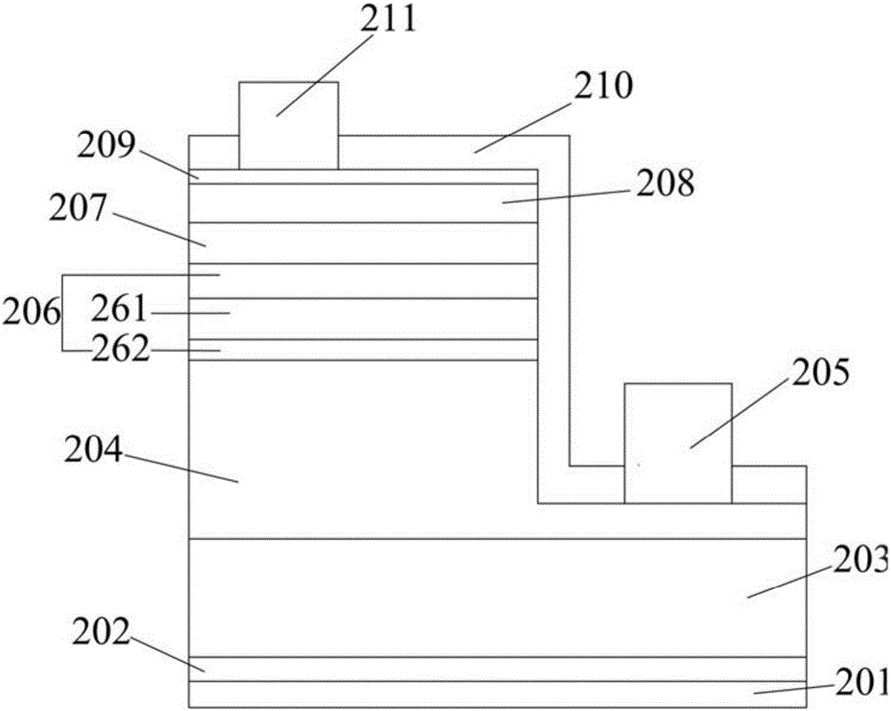
[0084] The growth method of conventional LED epitaxy is (see the epitaxial layer structure figure 1 ):
[0085] Step 101, processing the sapphire substrate: in a hydrogen atmosphere at 1000-1100°C, inject 100L / min-130L / min of H 2 , keep the reaction chamber pressure at 100-300mbar (mbar is the air pressure unit), and process the sapphire substrate for 5-10 minutes.
[0086] Step 102, grow low-temperature buffer layer GaN: lower the temperature to 500-600°C, keep the reaction chamber pressure at 300-600mbar, and feed NH at a flow rate of 10000-20000sccm (sccm remark standard milliliters per minute) 3 , 50-100sccm TMGa, 100L / min-130L / min H 2 1. Growing a low-temperature buffer layer GaN with a thickness of 20-40 nm on the sapphire substrate.
[0087] Step 103, corroding the low-temperature buffer layer GaN into an irregular island shape: raise the temperat...
PUM
| Property | Measurement | Unit |
|---|---|---|
| luminous efficiency | aaaaa | aaaaa |
Abstract
Description
Claims
Application Information