Oxygen-doped Sb nanometer phase change thin-film materials and preparation method thereof and application thereof

A thin film material, nanophase technology, applied in the fields of nanotechnology, nanotechnology, nanotechnology, etc. for materials and surface science, can solve the problem of long phase transition time, inability to meet the design requirements of high-speed PCRAM, and low thermal stability of materials. problems, to achieve the effect of improving stability, increasing storage speed, and reducing operating power consumption

Inactive Publication Date: 2017-02-15
JIANGSU UNIV OF TECH
View PDF5 Cites 7 Cited by
  • Summary
  • Abstract
  • Description
  • Claims
  • Application Information

AI Technical Summary

Problems solved by technology

[0003] Ge 2 Sb 2 Te 5 is currently the most studied phase change material, but Ge 2 Sb 2 Te 5 The thermal stability of the material is not high, the crystallization temperature is only about 160°C, and the temper

Method used


Image

  • Oxygen-doped Sb nanometer phase change thin-film materials and preparation method thereof and application thereof
  • Oxygen-doped Sb nanometer phase change thin-film materials and preparation method thereof and application thereof
  • Oxygen-doped Sb nanometer phase change thin-film materials and preparation method thereof and application thereof

Examples


Embodiment 1

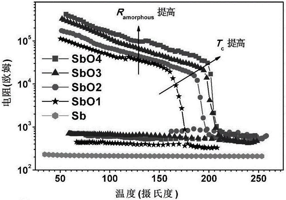
[0033] The structure of the oxygen-doped Sb nano phase change thin film material prepared in this embodiment is specifically represented as SbO1.

[0034] The preparation steps are:

[0035] 1. Clean the SiO2 / Si(100) substrate, clean the surface and back, remove dust particles, organic and inorganic impurities;

[0036] a) strong ultrasonic cleaning in acetone solution for 3-5 minutes, and rinse with deionized water;

[0037] b) Strong ultrasonic cleaning in ethanol solution for 3-5 minutes, rinse with deionized water, and dry the surface and back with high-purity N2;

[0038] c) Dry the water vapor in an oven at 120°C for about 20 minutes.

[0039] 2. Preparation of SbO by RF sputtering method 1 Film preparation:

[0040] a) The Sb sputtering target is installed, the purity of the target reaches 99.999% (atomic percentage), and the background vacuum is evacuated to 1×10 -4 Pa;

[0041] b) Set the sputtering power to 30W;

[0042] c) Using high-purity Ar and high-purity O...

Embodiment 2

[0048] Prepare the SbOx nano phase change thin film material of the present embodiment, its specific structure is respectively SbO 2 and SbO 3 and SbO 4 , and the SbO 2 and SbO 3 and SbO 4 The thickness of the nano phase change thin film material is 50nm.

[0049] The above SbO 2 and SbO 3 and SbO 4 The preparation method of nanometer phase-change film material is identical with example 1, just prepares SbO 2 The Ar gas flow rate set by the nano phase change thin film material is 28sccm, O 2 The flow rate is 2 sccm; the preparation of SbO 3 The Ar gas flow rate set by the nano phase change thin film material is 27sccm, O 2 The flow rate is 3 sccm; the preparation of SbO 4 The Ar gas flow set by the nano phase change thin film material is 26sccm, O 2 The flow rate is 4 sccm.


PUM

PropertyMeasurementUnit
Thicknessaaaaaaaaaa
Thicknessaaaaaaaaaa

Abstract

The present invention belongs to the semiconductor material field, and discloses the oxygen-doped Sb nanometer phase change thin-film materials. The chemical composition general formula is expressed by SbOx, wherein the Sb represents the Sb element, the O represents the nitrogen atom, the x represents different oxygen doping amount marks, and x=1,2,3 or 4. A magnetron sputtering method is employed for preparation, the substrate employs SiO2/Si(100) substrate, the target of sputter is the Sb target, the sputtering gas is high-purity Ar gas and the high-purity O2 gas, and the total flow of the argon and the oxygen is maintained to 30 sccm in the sputtering process. The oxygen-doped Sb materials can solve the defects and deficiencies of the pure Sb materials. Different oxygen atoms are doped to allow the Sb crystallization temperature to be obviously improved, the data maintenance capacity is enhanced, and the stability is improved. The RESET power consumption is reduced while the crystalline state resistance is improved.

Description

technical field [0001] The invention relates to a semiconductor material in the technical field of microelectronics, in particular to an antimony oxide nano film material used in a phase change memory and its preparation and application. Background technique [0002] The core of phase change memory (PCRAM) is chalcogenide-based phase change material, which has low resistance and high resistance in crystalline state and amorphous state respectively. Using the significantly different resistance values ​​as the "0" and "1" states of data storage, and relying on the Joule heat induced by electric pulses to achieve repeated conversions between high-resistance states and low-resistance states, the purpose of information storage can be achieved. Due to the advantages of small cell size, fast storage speed, low operating voltage, and low power consumption of PCRAM chips, with the development of semiconductor process technology to the nanometer level, the technical advantages of PCRA...

Claims


Application Information

Patent Timeline
IPC IPC(8): H01L45/00B82Y30/00
CPCB82Y30/00H10N70/8833H10N70/026
Inventor 胡益丰尤海鹏朱小芹邹华薛建忠张剑豪孙月梅吴世臣袁丽吴卫华郑龙翟良君
Owner JIANGSU UNIV OF TECH
Why Eureka
Try Eureka