Growth method for light-emitting diode epitaxial wafer

A technology for light emitting diodes and a growth method, which is applied to the growth field of light emitting diode epitaxial wafers, can solve the problems of reducing luminous efficiency, reducing the radiative recombination efficiency of electrons and holes, etc., so as to improve luminous efficiency, improve radiative recombination efficiency, and reduce polarization effect of effect

Active Publication Date: 2017-02-22
HC SEMITEK ZHEJIANG CO LTD
View PDF5 Cites 12 Cited by
  • Summary
  • Abstract
  • Description
  • Claims
  • Application Information

AI Technical Summary

Problems solved by technology

The electric field separates the electrons and holes in space, reduces the overlap between the electron wave function and the hole wave function, reduces the radiation recombination efficiency of electrons and holes, and greatly reduces the luminous efficiency of LEDs.

Method used


Image

  • Growth method for light-emitting diode epitaxial wafer
  • Growth method for light-emitting diode epitaxial wafer

Examples


Embodiment

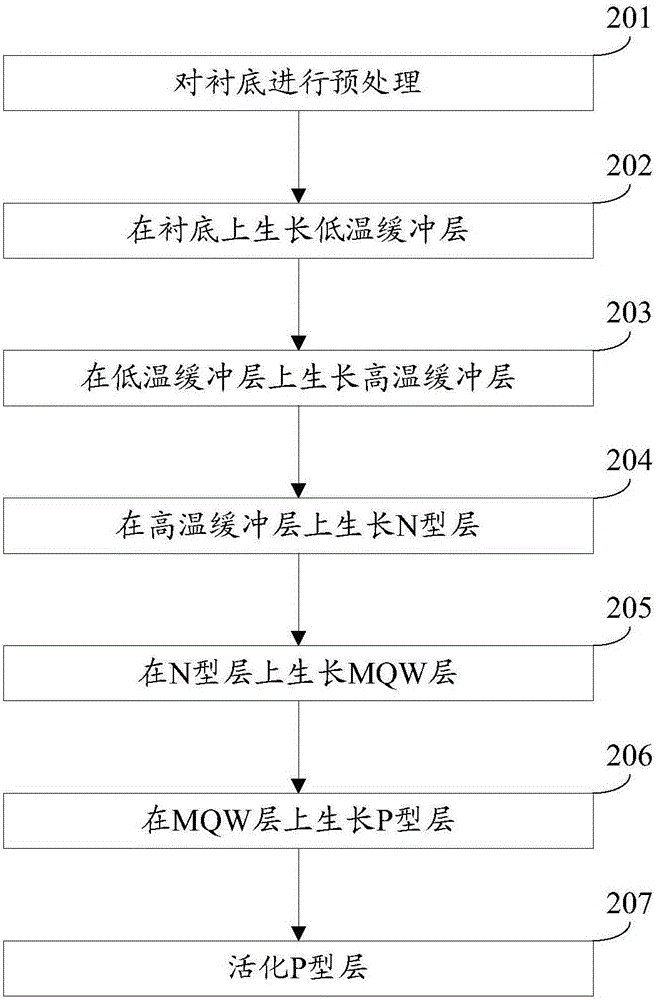
[0027] An embodiment of the present invention provides a method for growing a light-emitting diode epitaxial wafer. In this embodiment, Veeco K465i or C4 metal organic compound chemical vapor deposition (English: Metal Organic Chemical VaporDeposition, referred to as: MOCVD) equipment is used to realize the LED epitaxial wafer. growth method. Using high-purity hydrogen (H 2 ) or high-purity nitrogen (N 2 ) or high purity H 2 and high purity N 2 The mixed gas as the carrier gas, high-purity NH 3 As the N source, trimethylgallium (TMGa) and triethylgallium (TEGa) are used as the gallium source, trimethylindium (TMIn) is used as the indium source, silane (SiH4) is used as the N-type dopant, and trimethylaluminum ( TMAl) as an aluminum source, magnesium dicene (CP 2 Mg) as a P-type dopant. The pressure of the reaction chamber is controlled at 100-600 torr.

[0028] see figure 1 , the growth method includes:

[0029] Step 201: Perform pretreatment on the substrate.

[003...


PUM


Abstract

The invention discloses a growth method for a light-emitting diode epitaxial wafer, and belongs to the technical field of a semiconductor. The growth method comprises the steps of enabling a low-temperature buffer layer, a high-temperature buffer layer, an N type layer, an MQW layer and a P type layer to be grown on a substrate in sequence, wherein the MQW layer comprises an InGaN quantum well layer and a GaN quantum barrier layer which are laminated alternately; the quantum well layer comprises a first type quantum well, a second type quantum well, and a third type quantum well; the growth temperature of the quantum well layers in the first type quantum well is lowered layer by layer; the In content of the quantum well layers in the second type quantum well is changed layer by layer; the ratio of the In content to Ga content in the quantum well layers in the third type quantum well is decreased layer by layer; and the quantum well layers belong to the first type quantum well, the second type quantum well layer and the third type quantum well in the growth direction of the light-emitting diode epitaxial wafer in sequence. By adoption of the growth method, the overlapping degree of an electron wave function and a hole wave function can be effectively improved, and the light emitting efficiency of the LED is finally improved.

Description

technical field [0001] The invention relates to the technical field of semiconductors, in particular to a method for growing a light-emitting diode epitaxial wafer. Background technique [0002] A light-emitting diode (English: Light Emitting Diode, referred to as: LED) is a semiconductor electronic component that can emit light. As an efficient, environmentally friendly, and green new solid-state lighting source, LEDs are rapidly and widely used in traffic lights, automotive interior and exterior lights, urban landscape lighting, and mobile phone backlights. [0003] An existing LED epitaxial wafer includes a substrate, and a low-temperature buffer layer, a high-temperature buffer layer, an N-type layer, a multiple quantum well (Multiple Quantum Well, MQW for short) layer, and a P-type layer sequentially stacked on the substrate. Wherein, the MQW layer includes alternately stacked quantum well layers and quantum barrier layers, the growth conditions of each quantum well la...

Claims


Application Information

Patent Timeline
Patent Type & Authority Applications(China)
IPC IPC(8): H01L33/06H01L33/32H01L33/12H01L33/00
CPCH01L33/0075H01L33/06H01L33/12H01L33/325
Inventor 姚振从颖胡加辉
Owner HC SEMITEK ZHEJIANG CO LTD
Why Eureka
Try Eureka