Regulation and control method for electrical property of indium oxide nanofiber field effect transistor

A field effect transistor and nanofiber technology, which is applied in the field of transistor electrical performance regulation, can solve problems such as metal doping and the like that have not yet been seen, and achieve the effects of easy large-scale industrial production, broad application prospects, and simple and safe preparation process.

Inactive Publication Date: 2017-03-08
QINGDAO UNIV
View PDF0 Cites 20 Cited by
  • Summary
  • Abstract
  • Description
  • Claims
  • Application Information

AI Technical Summary

Problems solved by technology

However, no electrospinning method has been used to prepare metal-doped polycrystalline In 2 o 3 Semiconductor nanofibers, and related reports on the regulation of their electrical properties by changing the type and content of doped metals

Method used


Image

  • Regulation and control method for electrical property of indium oxide nanofiber field effect transistor
  • Regulation and control method for electrical property of indium oxide nanofiber field effect transistor
  • Regulation and control method for electrical property of indium oxide nanofiber field effect transistor

Examples


preparation example Construction

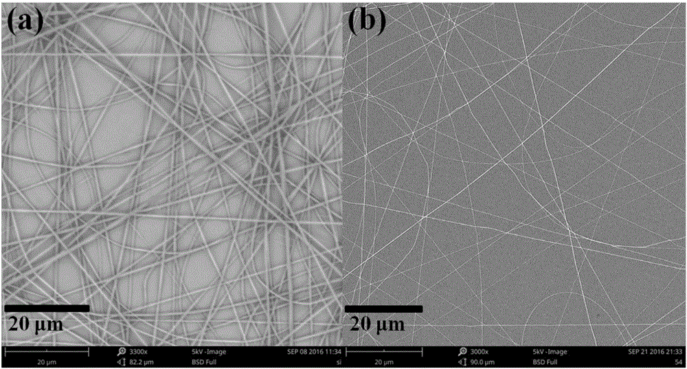
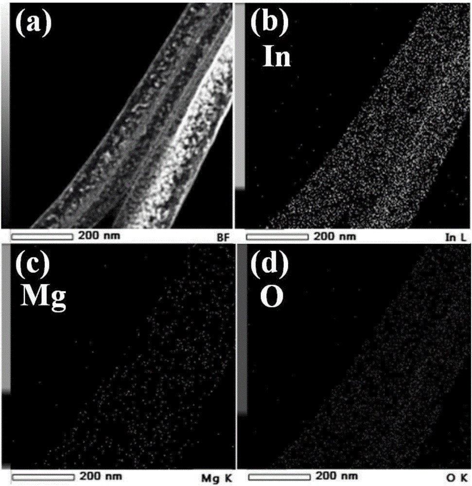
[0030] (3)In 2 o 3 Preparation of NFs and assembly of devices: extract 5ml of the solution prepared in step (1) or step (2), and pass the existing electrospinning technology (voltage 10-25kv, humidity 20-50%, the distance between the needle tip and the receiving substrate 10-20cm, solution propulsion speed 0.5-1ml / h) Spin the electrospinning precursor solution of pure In source or doped electrospinning precursor solution to cover the surface with 150-300nm SiO 2 In is prepared on a silicon wafer or ITO or FTO conductive glass with a dielectric layer 2 o 3 Nanofibers (In 2 o 3 NFs) or metal doped In 2 o 3 Nanofibers (In 2 o 3 NFs), and then attach the resulting In 2 o 3 Nanofibers (In 2 o 3 NFs) or metal doped In 2 o 3 Nanofibers (In 2 o 3 NFs) silicon wafers or conductive glass are baked on a baking table for 10-60 minutes, annealed by an ultraviolet lamp for 20-60 minutes, then placed in a muffle furnace for 400-600°C for 1-3 hours, and cooled naturally to Ta...

Embodiment 1

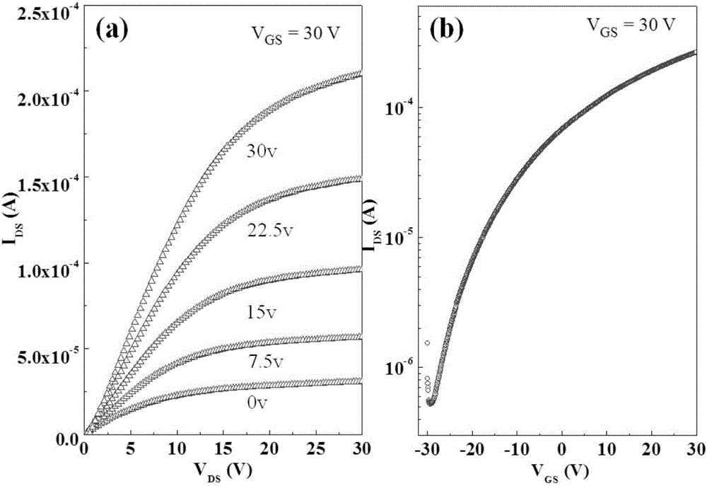
[0033] This example prepares In 2 o 3 The specific process of NFFETs is:

[0034] (1) Preparation of electrospinning precursor solution: 6g of polyvinylpyrrolidone (PVP), 0.8g of indium trichloride tetrahydrate, 40g of N, N-dimethylformamide (DMF) were mixed in a glass bottle, and magnetically The stirrer is fully stirred until the solution is uniform and transparent, forming a pure In source electrospinning precursor solution;

[0035] (2) Assembly of the device: extract 5ml of the pure In source electrospinning precursor solution prepared in step (1), and use the electrospinning technology (voltage 10-25kv, humidity 20-50%, the distance between the needle tip and the receiving substrate to be 10 -20cm, solution propulsion speed 0.5-1ml / h), the pure In source electrospinning precursor solution is spun to cover the surface with 150-300nm SiO 2 Dielectric layer silicon wafer or ITO or FTO conductive glass to get In 2 o 3 NFs, which will then be attached to In 2 o 3 The s...

Embodiment 2

[0037] This example prepares 2%-Mg doped In 2 o 3 The specific process of NFs and NFFETs is:

[0038] (1) Preparation of electrospinning precursor solution: 6g of polyvinylpyrrolidone (PVP), 0.8g of indium trichloride tetrahydrate, 40g of N, N-dimethylformamide (DMF) were mixed in a glass bottle, and magnetically The stirrer is fully stirred until the solution is uniform and transparent, forming a pure In source; electrospinning precursor solution;

[0039] (2) Preparation of doped electrospinning precursor solution: take 0.016 g of magnesium chloride hexahydrate and dissolve it in the electrospinning precursor solution of pure In source configured in step 1 to form a doped Mg doping ratio of 2 wt%. Electrospinning precursor solution;

[0040] (3) Assembly of the device: extract 5ml of the doped electrospinning precursor solution prepared in step (2), and use electrospinning technology (voltage 15kv, humidity 30%, distance from needle tip to receiving substrate 15cm, soluti...


PUM

PropertyMeasurementUnit
lengthaaaaaaaaaa
widthaaaaaaaaaa

Abstract

The invention belongs to the regulation and control technical field of electrical property of a transistor, and relates to a regulation and control method for electrical property of an indium oxide nanofiber field effect transistor. In<2>O<3> nanofibers are prepared through a simple, convenient and low-cost electrospinning technology; the electrical property of the In<2>O<3> nanofiber field effect transistor is regulated and controlled through simple and feasible metal doping so as to regulate and control the electrical property, such as a threshold voltage, an off-state current, a switching ratio and the like, of the In<2>O<3> nanofiber field effect transistor in a simple and convenient, efficient and low-cost manner, in order to obtain the excellent-performance and metal-doped In<2>O<3> nanofiber field effect transistor; the preparation process is simple, convenient, and safe, and the principle is reliable, and the production cost is low; and the prepared In<2>O<3> nanofibers and the metal-doped In<2>O<3> nanofibers have wide application prospect in the fields of an electronic switching device, a display, biological and chemical sensors and the like, and large-scale industrial production can be performed easily.

Description

[0001] Technical field: [0002] The invention belongs to the technical field of transistor electrical performance regulation and relates to an indium oxide nanofiber field effect transistor (In 2 o 3 NFFETs) electrical performance control method, the use of main group metal elements (Mg, Al, Ga) or transition metal elements (Y, Sr, Sc, etc.) for simple doping to control In 2 o 3 The electrical properties of NFFETs can be widely used in high-performance displays, optoelectronic devices, detectors, rectifiers and other fields. [0003] Background technique: [0004] Compared with bulk and thin-film materials, one-dimensional semiconductor materials can effectively improve the optoelectronic properties of devices due to their advantages such as directional electron transport paths, lower material cost, large specific surface area, and excellent mechanical properties. At present, the methods for preparing one-dimensional materials mainly include chemical vapor deposition (CVD),...

Claims


Application Information

Patent Timeline
Patent Type & Authority Applications(China)
IPC IPC(8): H01L29/775H01L21/02D01F9/08D01F1/10B82Y10/00
CPCB82Y10/00D01F1/10D01F9/08H01L21/02565H01L21/02628H01L29/775
Inventor 王凤云张洪超宋龙飞罗麟氍
Owner QINGDAO UNIV
Why Eureka
Try Eureka