Gas-liquid interface processing method for a semiconductor gas sensor

A gas sensor and processing method technology, applied in the direction of material resistance, etc., can solve the problems of difficult repeated batch production, unstable properties of gas sensors, etc., and achieve the effects of simple process, good gas response and recovery performance, easy operation and mass production

Active Publication Date: 2019-08-20
SOUTH CHINA NORMAL UNIVERSITY
View PDF7 Cites 0 Cited by
  • Summary
  • Abstract
  • Description
  • Claims
  • Application Information

AI Technical Summary

Problems solved by technology

[0003] The invention provides a gas-liquid interface processing method and product of a semiconductor gas sensor, which are used to solve the problem that the properties of the gas sensor prepared in the prior art are unstable and difficult to repeat batch production

Method used


Image

  • Gas-liquid interface processing method for a semiconductor gas sensor
  • Gas-liquid interface processing method for a semiconductor gas sensor
  • Gas-liquid interface processing method for a semiconductor gas sensor

Examples


Embodiment 1

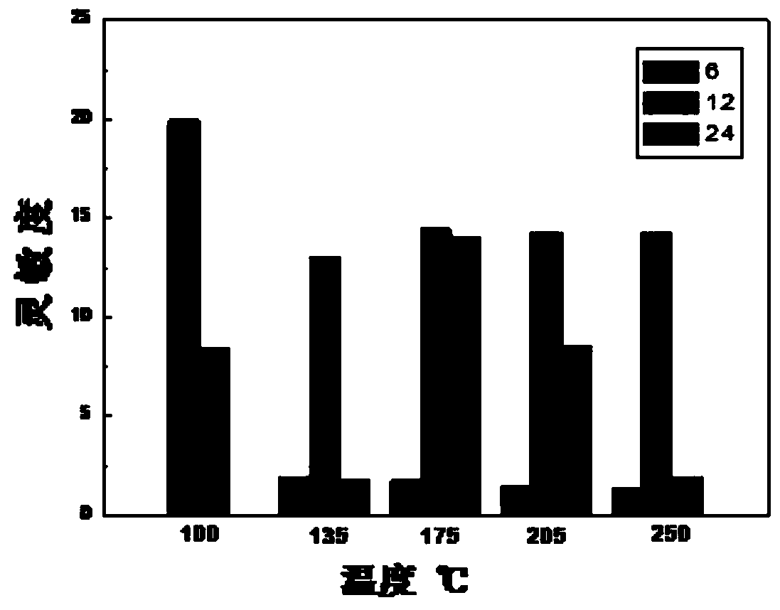
[0028] Add 0.025mol / l cadmium sulfate and 0.025mol / l sodium thiosulfate into 200ml deionized water for ultrasonic dissolution to obtain a cadmium precursor;

[0029] Cover the petri dish with plastic wrap, transfer it to a dark room, and place it under two 8W, 254nm ultraviolet lamps for a certain period of time;

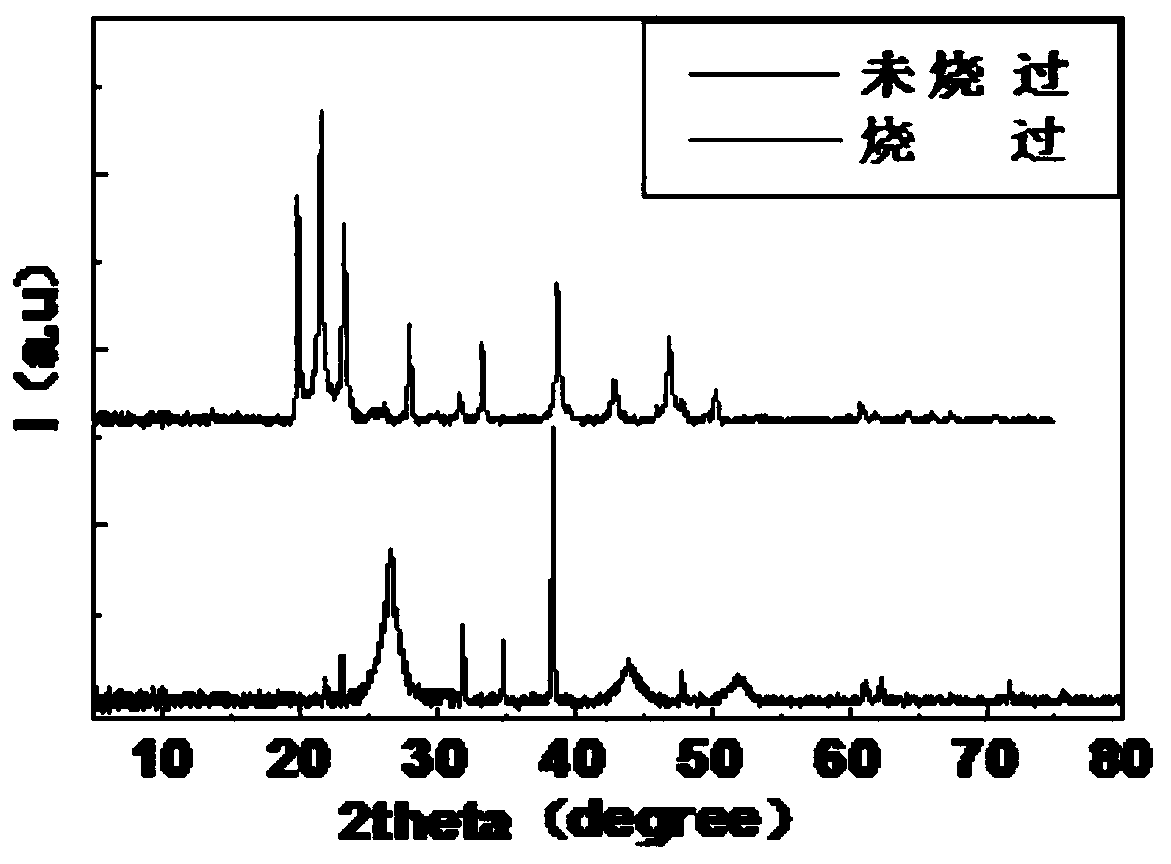
[0030] After reacting for 24 hours, use a clean glass piece to pick up the film on the surface;

[0031] Float the film to the surface of deionized water, let it stand for 0.1 hour, pick it up gently with a ceramic tube, and then dry it at 60°C to obtain cadmium-rich cadmium sulfide nanotubes;

[0032] The ceramic tube was welded on the base, loaded with resistance wire, and heat-treated at 180°C for 0.5 hours to obtain a cadmium oxide-cadmium sulfide composite film gas sensor.

Embodiment 2

[0034] Add 0.2mol / l cadmium sulfate and 0.1mol / l sodium thiosulfate into 200ml deionized water for ultrasonic dissolution to obtain a cadmium precursor;

[0035] Cover the petri dish with plastic wrap, transfer it to a dark room, and place it under two 8W, 254nm ultraviolet lamps for a certain period of time;

[0036] After reacting for 12 hours, use a clean glass piece to pick up the film on the surface;

[0037] Float the film to the surface of deionized water, let it stand for 0.25 hours, pick it up gently with a ceramic tube, and then dry it at 60°C to obtain cadmium-rich cadmium sulfide nanotubes;

[0038] The ceramic tube was welded on the base, loaded with resistance wire, and heat-treated at 200°C for 0.8 hours to obtain a cadmium oxide-cadmium sulfide composite film gas sensor.

Embodiment 3

[0040] Add 1.2mol / l cadmium sulfate and 0.2mol / l sodium thiosulfate into 200ml deionized water for ultrasonic dissolution to obtain a cadmium precursor;

[0041] Cover the petri dish with plastic wrap, transfer it to a dark room, and place it under two 8W, 254nm ultraviolet lamps for a certain period of time;

[0042] After reacting for 6 hours, use a clean glass piece to pick up the film on the surface;

[0043] Float the film on the surface of deionized water, let it sit for fifteen minutes, then gently pick it up with a ceramic tube, and then dry it at 60°C to obtain cadmium-rich cadmium sulfide nanotubes;

[0044] The ceramic tube was welded on the base, loaded with resistance wire, and heat treated at 250°C for 1 hour to obtain a cadmium oxide-cadmium sulfide composite thin film gas sensor.

[0045] Cadmium sulfate can obtain a cadmium sulfide layer with a certain thickness and uniformity at a concentration of 0.025mol / l-1.2mol / l at 25°C. If the concentration is too sma...


PUM

PropertyMeasurementUnit
diameteraaaaaaaaaa

Abstract

The invention proposes a gas-liquid interface processing method for a semiconductor gas sensor comprising the following steps: preparing a precursor solution; irradiating the precursor solution with ultraviolet light to prepare a film on the surface of the solution; picking up the surface film with a clean glass sheet and transferring it to Wash the film on the surface of deionized water; pick up the film cleaned by deionized water with a ceramic tube; weld the ceramic tube with the film on the special base of the gas sensor, and there is a heating resistance wire in the ceramic tube; insert the base into the On the gas-sensing test system, apply a voltage to the resistance wire, and obtain a gas sensor after obtaining a film with stable composition. The invention achieves the attachment of gas-sensitive materials on the sensor substrate, improves the defects of multi-step operation, high-temperature processing, stability, repeated processing and batch processing in the current gas sensor processing process, and has the advantages of easy-to-obtain raw materials, simple process, It is characterized by easy operation and mass production, good gas response and recovery performance and excellent stability.

Description

technical field [0001] The invention relates to a gas-liquid interface processing method for a semiconductor gas sensor. Background technique [0002] Gas sensors play an important role in environmental detection. Resistive semiconductor gas sensors are currently the most widely used type of gas sensors in the market, accounting for about 85% of the market share. The basic processing methods are as follows: First, various methods are used to prepare powder material; secondly, the powder material is coated into a slurry; subsequently, the slurry is manually coated on a ceramic substrate (the current substrate is mainly a ceramic tube) and calcined to solidify the coating; finally, the ceramic tube is welded on the base Complete sensor processing. Obviously, there are several obvious problems in the sensor processing technology with manual coating as the core: first, the operation is cumbersome; second, the film is obtained by manual coating, and there is too much physical co...

Claims


Application Information

Patent Timeline
Patent Type & Authority Patents(China)
IPC IPC(8): G01N27/12
Inventor 孙丰强陈颖
Owner SOUTH CHINA NORMAL UNIVERSITY
Why Eureka
Try Eureka