Back contact solar cell string and preparation method thereof, component and system
A technology for solar cells and back-contact cells, applied in the field of solar cells, can solve the problems of difficult alignment and welding of cells, large number of emitter and base electrodes, and large power loss, so as to reduce lateral transmission loss and improve filling factor. , The effect of saving the cost of silver paste
- Summary
- Abstract
- Description
- Claims
- Application Information
AI Technical Summary
Problems solved by technology
Method used
Image
Examples
Embodiment 1
[0050] A method for preparing a back-contact solar cell string in this embodiment includes the following steps:
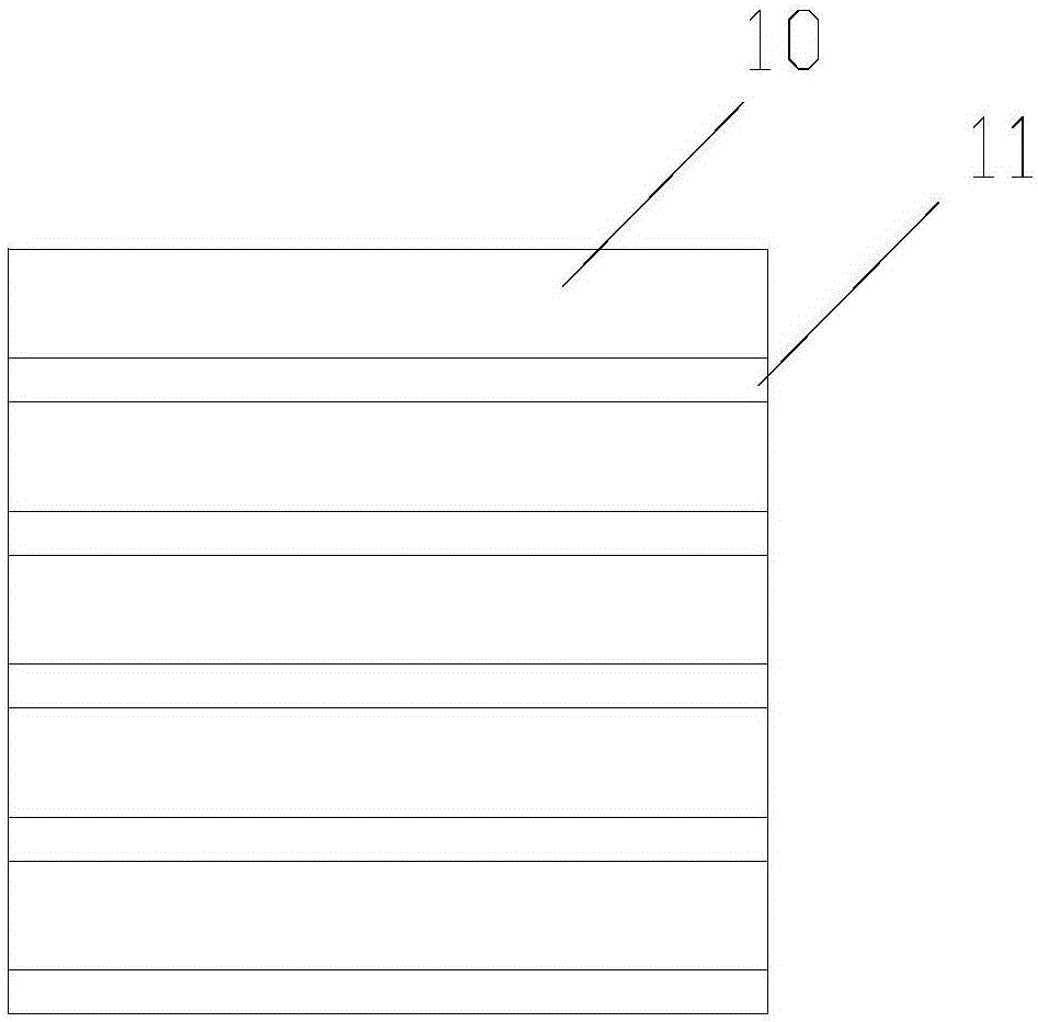
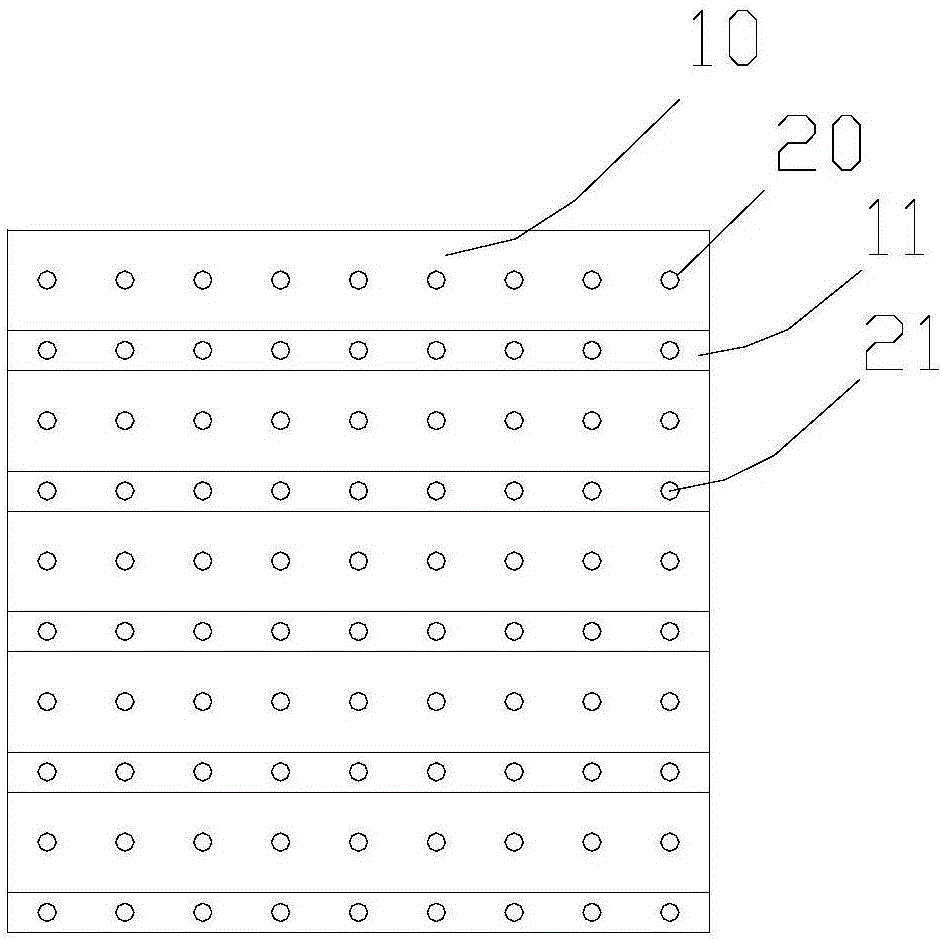
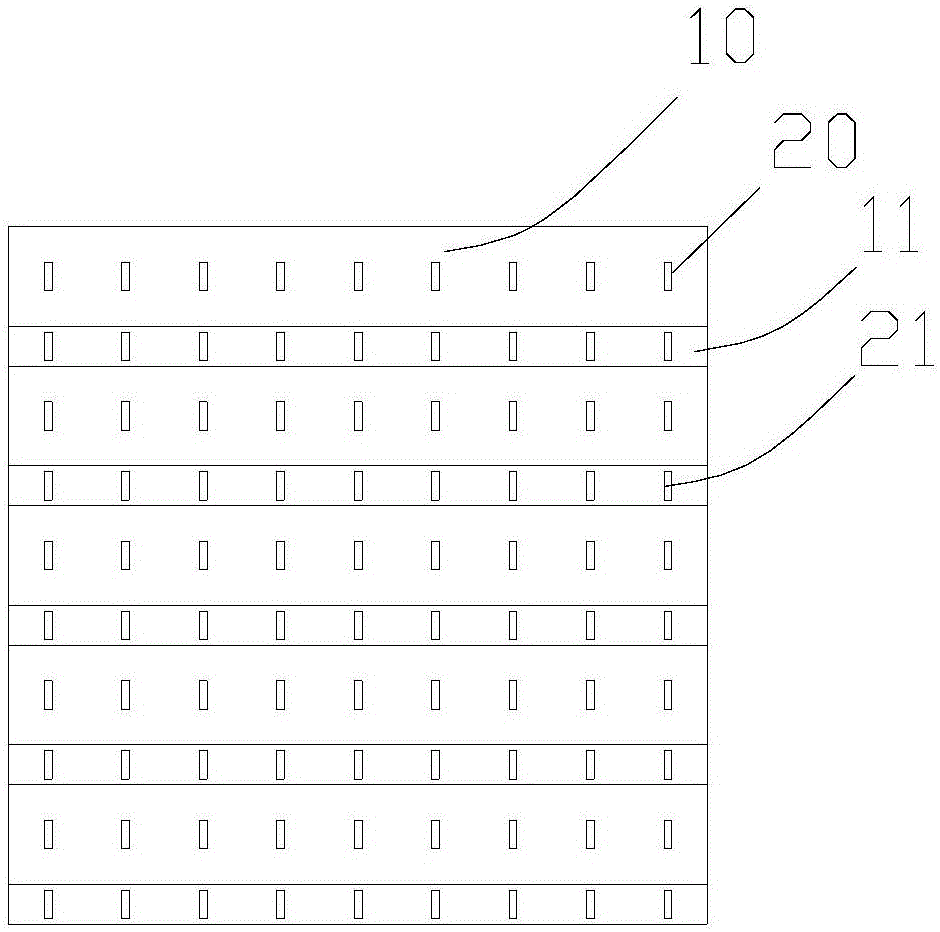
[0051] (1) Prepare a back-contact solar cell in which emitter p+ regions 10 and base n+ regions 11 are alternately arranged on the back surface of a silicon wafer. In this embodiment, an N-type single crystal silicon substrate is selected, and the resistivity is 1-30Ω·cm. The thickness is 50-300μm, and the N-type crystalline silicon substrate is subjected to surface texture treatment before use, and then the emitter p+ region 10 and the base n+ region 11 are alternately arranged by using diffusion or ion implantation, masking, etching and other technologies on the back surface of the battery. Then use dielectric films such as silicon oxide, silicon nitride and aluminum oxide to passivate the back surface of the battery, passivate the front surface and optical antireflection, so as to form the required emitter p+ regions 10 and base n+ regions 11 alternately Solar ...
Embodiment 2
[0058] A method for preparing a back-contact solar cell string in this embodiment includes the following steps:
[0059] Steps (1)-(3) and (5) are the same as those in Embodiment 1, and will not be repeated here.
[0060] (3)', print solder paste on the emitter segment electrode 20 of the narrow strip-shaped back contact battery after step 3 to form the emitter thermosensitive conductive layer 30, and print solder paste on the base segment electrode 21 to form the base thermally sensitive conductive layer 31 . The overink pattern of solder paste can be circular or linear. Its width cannot exceed the width of the doped region in which it is located. During printing, the emitter thermally sensitive conductive layer 30 after ink must be located on the emitter segment electrode 20 , and the base thermally sensitive conductive layer 31 after ink is located on the base segment electrode 21 . The enlarged picture of the local structure after printing is as follows Figure 6 As sh...
PUM
 Abstract
Description
Claims
Application Information


