Epitaxial wafer of light-emitting diode and growth method thereof

A technology of light-emitting diodes and growth methods, applied in the field of epitaxial wafers of light-emitting diodes and their growth, can solve problems such as dislocations that are difficult to eliminate, screw dislocation lattices, defects, etc., to improve internal quantum efficiency and antistatic ability, improve The effect of crystal quality and growth temperature improvement

Active Publication Date: 2017-05-10
HC SEMITEK ZHEJIANG CO LTD
View PDF4 Cites 12 Cited by
  • Summary
  • Abstract
  • Description
  • Claims
  • Application Information

AI Technical Summary

Problems solved by technology

[0005] Although the buffer layer composed of three-dimensional island-shaped grains can improve the lattice matching between GaN and the substrate, growing the buffer layer at low temperature and low pressure can easily lead to lattice defects

Method used


Image

  • Epitaxial wafer of light-emitting diode and growth method thereof
  • Epitaxial wafer of light-emitting diode and growth method thereof
  • Epitaxial wafer of light-emitting diode and growth method thereof

Examples


Embodiment 1

[0028] An embodiment of the present invention provides an epitaxial wafer of a light emitting diode, see figure 1 , the epitaxial wafer includes a substrate 1 , and a buffer layer 2 , an undoped GaN layer 3 , an N-type GaN layer 4 , a light emitting layer 5 , and a P-type GaN layer 6 stacked on the substrate 1 in sequence.

[0029] In this embodiment, the buffer layer is doped with Mg.

[0030] Specifically, the doping concentration of Mg in the buffer layer is smaller than the doping concentration of the P-type dopant in the P-type GaN layer.

[0031] Optionally, the buffer layer may include one of GaN layers, AlGaN layers, InGaN layers, AlInGaN layers, alternately stacked InGaN layers, and AlGaN layers.

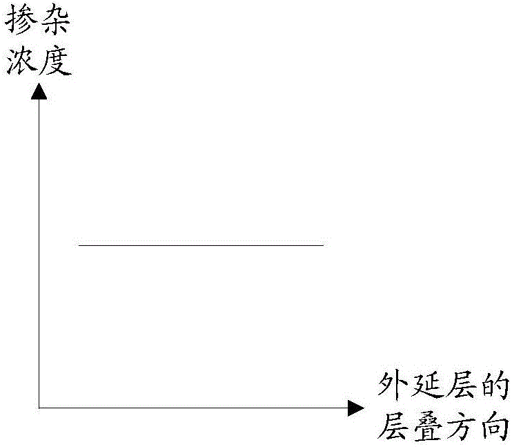
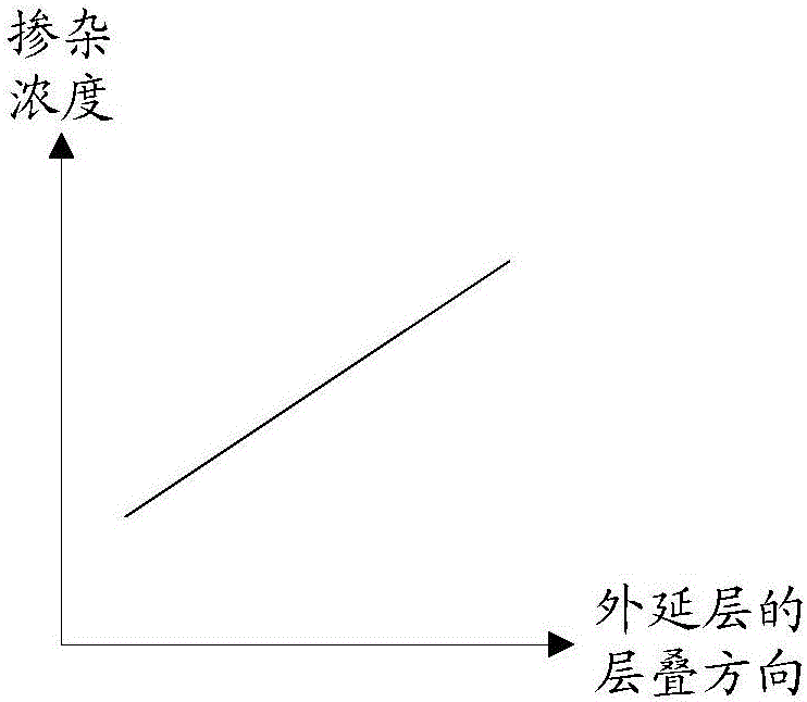
[0032] Optionally, the doping concentration of Mg in the buffer layer can be changed in one of the following ways: remain unchanged (such as Figure 2a shown), gradually increasing along the stacking direction of the epitaxial wafer (such as Figure 2b shown), and gradua...

Embodiment 2

[0045] An embodiment of the present invention provides a method for growing an epitaxial wafer of a light emitting diode, which is suitable for growing the epitaxial wafer provided in Embodiment 1. Realized using high-purity H 2 or N 2 As carrier gas, TMGa, TMAl, TMIn and NH 3 As Ga source, Al source, In source and N source respectively, using SiH 4 and Cp 2 Mg is used as an N-type dopant and a P-type dopant respectively, and metal-organic chemical vapor deposition equipment or other equipment is used to complete the growth of epitaxial wafers.

[0046] Specifically, see Figure 4 , the growth method includes:

[0047] Step 201: growing a buffer layer on a substrate.

[0048] In this embodiment, the buffer layer is doped with Mg.

[0049]Specifically, the doping concentration of Mg in the buffer layer is smaller than the doping concentration of the P-type dopant in the P-type GaN layer.

[0050] Optionally, the buffer layer may include one of GaN layers, AlGaN layers, ...


PUM

PropertyMeasurementUnit
Thicknessaaaaaaaaaa
Thicknessaaaaaaaaaa
Temperatureaaaaaaaaaa

Abstract

The invention discloses an epitaxial wafer of a light-emitting diode and a growth method thereof, and belongs to the technical field of semiconductors. The epitaxial wafer comprises a substrate, and a buffer layer, a non-doped GaN layer, an N-type GaN layer, a light-emitting layer and a P-type GaN layer which are laminated on the substrate in turn. Mg is doped in the buffer layer. According to the epitaxial wafer, Mg is doped in the buffer layer, Mg can induce the material of the buffer layer to three-dimensional growth from two-dimensional growth to form three-dimensional island crystal grains with no requirement for the growth mode of low temperature and low pressure of the buffer layer, and the growth temperature of the buffer layer can be increased so that edge dislocation, screw dislocation and other lattice defects can be reduced, the crystal quality of the epitaxial wafer can be enhanced and the internal quantum efficiency and the anti-static capacity of the LED can be enhanced. Besides, the non-doped GaN layer is arranged between the buffer layer and the N-type GaN layer, and the non-doped GaN layer has the effect of separation so as to avoid the influence of the doped Mg in the buffer layer on electron injection light-emitting layer composite luminescence of the N-type GaN layer.

Description

technical field [0001] The invention relates to the technical field of semiconductors, in particular to an epitaxial wafer of a light emitting diode and a growth method thereof. Background technique [0002] The semiconductor light-emitting diode (English: Light Emitting Diode, referred to as: LED) represented by gallium nitride has excellent characteristics such as large band gap, high electron saturation drift speed, high temperature resistance, and high power capacity. Its ternary alloy InGaN The band gap is continuously adjustable from 0.7ev to 3.4ev, and the emission wavelength covers the entire region of visible light and ultraviolet light, which has broad prospects in the emerging optoelectronic industry. [0003] GaN-based LED epitaxial wafers are epitaxially grown on heterogeneous substrates (such as sapphire substrates), and the lattice mismatch between GaN and the substrate is large. In order to improve the lattice matching between GaN and the substrate, a buffer...

Claims


Application Information

Patent Timeline
IPC IPC(8): H01L33/32H01L33/30H01L33/00
CPCH01L33/007H01L33/305H01L33/325
Inventor 刘华容
Owner HC SEMITEK ZHEJIANG CO LTD
Why Eureka
Try Eureka