Low-temperature polycrystalline silicon film, preparation method thereof, thin film transistor and display panel

A low-temperature polysilicon and thin-film technology, applied in the direction of transistors, electric solid-state devices, semiconductor devices, etc., can solve the problems of reducing the electrical performance of thin-film transistors, increasing the leakage current of thin-film transistors, and the instability of threshold voltage of thin-film transistors. Current, the effect of improving electrical performance

Active Publication Date: 2017-06-13
BOE TECH GRP CO LTD
View PDF8 Cites 6 Cited by
  • Summary
  • Abstract
  • Description
  • Claims
  • Application Information

AI Technical Summary

Problems solved by technology

Due to the small grain size of low-temperature polysilicon, there are many grain boundaries of low-temperature polysilicon in the active layer, which increases the leakage current when th

Method used


Image

  • Low-temperature polycrystalline silicon film, preparation method thereof, thin film transistor and display panel
  • Low-temperature polycrystalline silicon film, preparation method thereof, thin film transistor and display panel
  • Low-temperature polycrystalline silicon film, preparation method thereof, thin film transistor and display panel

Examples


Embodiment 1

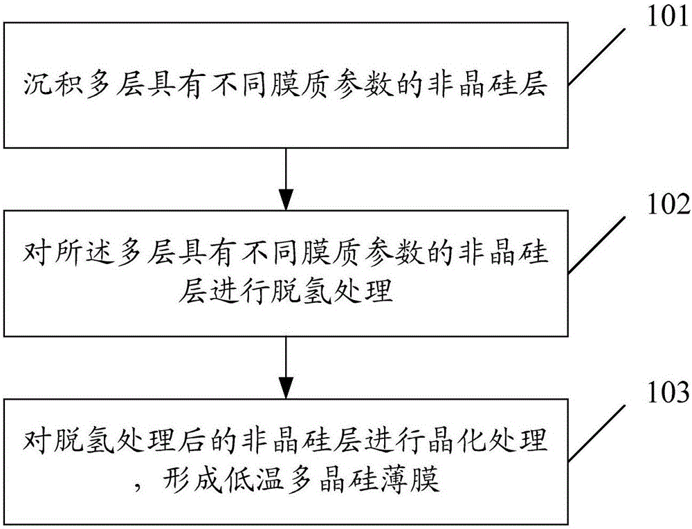
[0034] Such as figure 1 As shown, the preparation method of the low-temperature polysilicon thin film of embodiment one of the present invention comprises:

[0035] Step 101, depositing multiple layers of amorphous silicon layers with different film quality parameters; wherein the film quality parameters include refractive index parameters and / or thermal conductivity parameters;

[0036] Step 102, performing dehydrogenation treatment on the multi-layer amorphous silicon layers with different film quality parameters;

[0037] Step 103, performing crystallization treatment on the dehydrogenated amorphous silicon layer to form a low-temperature polysilicon film.

[0038] In the embodiment of the present invention, by depositing multiple layers of amorphous silicon layers with different film quality parameters, the refractive index and thermal conductivity of amorphous silicon with different film quality parameters are different, which is conducive to forming a uniform 400-500nm ...

Embodiment 2

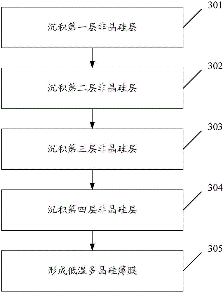
[0058] Such as image 3 and Figure 4 As shown, this embodiment takes depositing four layers of amorphous silicon layers as an example, including the following steps:

[0059] 301, depositing the first layer of amorphous silicon layer

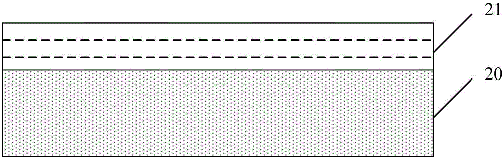
[0060] In this step, the first layer of amorphous silicon layer 211 (also called amorphous silicon film) is deposited on the buffer layer 20. The deposition temperature of this layer of amorphous silicon layer is the lowest, and the gas flow ratio is the smallest (SiH 4 / H 2 ), under this condition, the formed amorphous silicon layer has a small refractive index, a small thermal conductivity, and a relatively loose film quality.

[0061] 302, depositing a second amorphous silicon layer

[0062] This step is to change the PECVD process parameters after step 301 is completed, continue to deposit the second layer of amorphous silicon layer 212 on the surface of the first layer of amorphous silicon, the layer deposition temperature increases, a...

application example 1

[0072] Deposit 50nm and 300nm SiN on glass substrates using PECVD process x and SiO 2 Form SiN x and SiO 2 Double buffer layer. Use PECVD process to deposit nano-silicon thin film layer on the double buffer layer, the reaction gas is silane (SiH 4 ) and hydrogen (H 2 ), wherein, the first layer of amorphous silicon deposition parameters, the gas flow of silane is 140sccm, the gas flow of hydrogen is 1200sccm, the radio frequency power is 120W; the working pressure is 290Pa; the temperature is 370°C; the deposition time is 20 seconds. Then change the PECVD parameters to carry out the second layer of amorphous silicon deposition, the second layer of amorphous silicon deposition parameters, the gas flow of silane is 160sccm, the gas flow of hydrogen is 1200sccm, the radio frequency power is 120W; the working pressure is 290Pa, the temperature is 390°C, The deposition time was 20 seconds. Continue to change the PECVD parameters to carry out the third layer of amorphous silic...


PUM


Abstract

The invention discloses a low-temperature polycrystalline silicon film, a preparation method thereof, a thin film transistor and a display panel. The preparation method of the low-temperature polycrystalline silicon film comprises the steps that multiple non-crystalline silicon layers having different membranous parameters deposit, wherein the membranous parameters include refractive index parameters and/or heat conductivity coefficient parameters; dehydrogenation treatment is conducted on the multiple non-crystalline silicon layers having different membranous parameters; crystallization treatment is conducted on the non-crystalline silicon layers subjected to the dehydrogenation treatment to form the low-temperature polycrystalline silicon film. According to the embodiment, by depositing the multiple non-crystalline silicon layers having different membranous parameters different in non-crystalline silicon refraction index and heat conductivity coefficient, formation of large-sized crystalline grains in the crystallization process is promoted, active layer low-temperature polycrystalline silicon has fewer crystal boundaries, leaked current during connection of the thin film transistor can be decreased, and the electrical performance of the thin film transistor is improved.

Description

technical field [0001] This application relates to but not limited to the field of display technology, especially a low-temperature polysilicon thin film and its preparation method, a thin film transistor and a display panel. Background technique [0002] Liquid Crystal Display (LCD) is a display that uses liquid crystal to control light transmittance technology to achieve color. The current liquid crystal display is mainly a thin film transistor (Thin Film Transistor, TFT) liquid crystal display. [0003] Organic light-emitting display (OLED) is an active light-emitting device. Organic light-emitting display has attracted much attention due to its many advantages such as self-luminescence, fast response, thinness, low power consumption and flexible display. It is considered to be the next generation of flat panel display technology. In the organic light emitting display technology, thin film transistors are required to drive the organic light emitting display to emit light...

Claims


Application Information

Patent Timeline
IPC IPC(8): H01L21/02C23C16/44C23C16/52H01L29/786H01L27/32G02F1/1362
CPCH01L29/78672G02F1/1362H01L21/02532H01L21/0262C23C16/44C23C16/52H10K59/12
Inventor 杨昕
Owner BOE TECH GRP CO LTD
Why Eureka
Try Eureka