Back structure of electron multiplying charge-coupled device (EMCCD) and production method of back structure

A charge-coupled device and backside structure technology, applied in the direction of electric solid-state devices, electrical components, semiconductor devices, etc., can solve the problems of less device solutions, chip cracking, high cost, etc., and achieve improved light response time, uniform and effective removal, and reduced stress The effect of action

Pending Publication Date: 2017-06-13
NORTH ELECTRON RES INST ANHUI CO LTD
View PDF4 Cites 3 Cited by
  • Summary
  • Abstract
  • Description
  • Claims
  • Application Information

AI Technical Summary

Problems solved by technology

However, the current domestic research on the back structure of electron multiplier charge-coupled devices is still in the research and development stage, and the cost and process have not yet been achieved to achieve a suitable balance
At present, the mainstream backside structure manufacturing method requires multi-step adjustment of process parameters during grinding and polishing, whi

Method used


Image

  • Back structure of electron multiplying charge-coupled device (EMCCD) and production method of back structure
  • Back structure of electron multiplying charge-coupled device (EMCCD) and production method of back structure
  • Back structure of electron multiplying charge-coupled device (EMCCD) and production method of back structure

Examples


Embodiment Construction

[0033] Embodiments of the present invention will be further described in detail below in conjunction with the accompanying drawings.

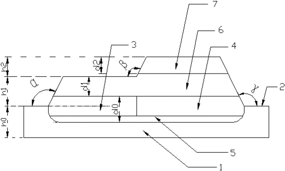
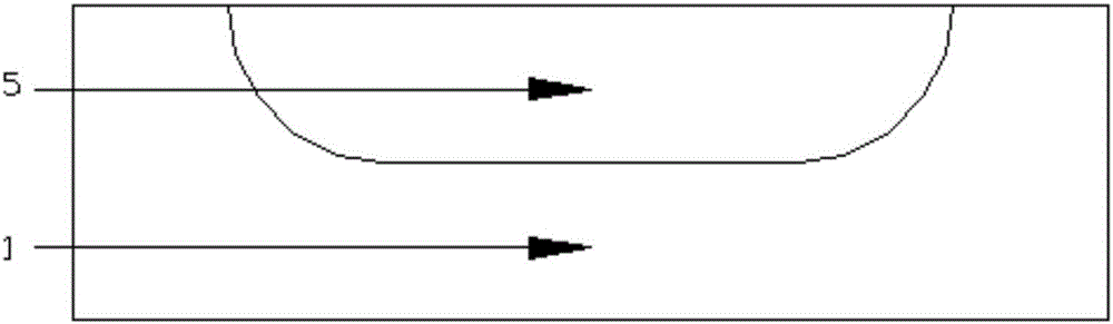
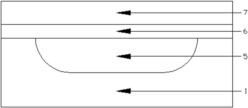
[0034] Such as figure 1 Shown in the structure schematic diagram of the present invention: a kind of EMCCD chip back structure comprises EMCCD chip 1, electrode lead-out area 2 of EMCCD chip 1, photosensitive area 3, storage gain area 4, ion implantation area 5, anti-reflection film 6 and metal shielding layer 7. Electrode extraction region 2, photosensitive region 3 and storage gain region 4 are adjacently formed in the backside silicon body of EMCCD chip 1, ion implantation region 5 is formed in photosensitive region 3 and storage gain region 4 by low-energy ion implantation, and in photosensitive region 3 An anti-reflection film 6 is coated on the surface, and an anti-reflection film 6 and a metal shielding layer 7 are provided on the surface of the storage gain area 4 .

[0035] The electrode lead-out area 2 is arranged on both sides of t...


PUM

PropertyMeasurementUnit
Thicknessaaaaaaaaaa
Thicknessaaaaaaaaaa

Abstract

The invention relates to a back structure of an electron multiplying charge-coupled device (EMCCD) and a production method of the back structure. The back structure comprises an EMCCD chip, electrode extracting regions, a photosensitive region, a storage grain region, ion implanting regions, an antireflection film and a metal shielding layer, wherein the electrode extracting regions are arranged on two sides of the back side of the EMCCD chip; bonding graphs are arranged on the electrode extracting regions at intervals; the photosensitive region and the storage grain region on the back side of the EMCCD chip are positioned between the electrode extracting regions; the ion implanting regions formed by implanting low-energy ions are separately formed inside the photosensitive region and the storage grain region; by using the antireflection film on the surface of the photosensitive region, a standing wave effect can be reduced, and reflected light rays are reduced; by using the metal shielding layer on the surface of the storage grain region, transmission of incident light on the surface of the storage grain region can be prevented. The back structure disclosed by the invention can be used for improving the photoelectric conversion efficiency of the EMCCD; meanwhile, the manufacturing cost of the device also can be reduced, and the rate of finished products is improved.

Description

technical field [0001] The invention relates to a back structure of an electron multiplying charge-coupled device and a manufacturing method thereof, belonging to the technical field of charge-coupled devices. Background technique [0002] After years of development, electron multiplying charge-coupled devices (EMCCDs) have been widely used in image scanning, industrial non-contact measurement, aerospace, astronomical remote sensing, military, medical and many other fields. Electron multiplying charge-coupled device is a large-scale integrated optoelectronic device, which has the functions of photoelectric conversion, charge storage, charge transfer, charge measurement, etc., and also has technical characteristics such as high sensitivity, high signal-to-noise ratio, high modulation transfer function, and all solid state. No matter in the technical upgrading of the traditional daytime digital imaging industry, such as X-ray digital imaging systems, various high frame rate ca...

Claims


Application Information

Patent Timeline
IPC IPC(8): H01L27/148
CPCH01L27/148H01L27/14806
Inventor 刘庆飞陈计学赵建强朱小燕赵绢
Owner NORTH ELECTRON RES INST ANHUI CO LTD
Why Eureka
Try Eureka