Thin-film transistor structure visible blind photodetector and preparation method thereof

A technology of thin film transistors and photodetectors, applied in semiconductor devices, sustainable manufacturing/processing, circuits, etc., can solve the problems of low UV-visible light suppression ratio, high preparation cost, complicated process, etc., and achieve high suppression ratio and excellent preparation process Simple, enhanced photoelectric response effect

Active Publication Date: 2018-07-10
NINGBO INST OF MATERIALS TECH & ENG CHINESE ACADEMY OF SCI
View PDF7 Cites 0 Cited by
  • Summary
  • Abstract
  • Description
  • Claims
  • Application Information

AI Technical Summary

Problems solved by technology

At present, thin-film transistor ultraviolet photodetectors with high photoresponsivity and high sensitivity have been reported, but there are still problems such as small ultraviolet-visible light suppression ratio, high preparation cost, and complicated process.

Method used


Image

  • Thin-film transistor structure visible blind photodetector and preparation method thereof
  • Thin-film transistor structure visible blind photodetector and preparation method thereof
  • Thin-film transistor structure visible blind photodetector and preparation method thereof

Examples


preparation example Construction

[0032] FIG. 2 is a flow chart of a method for fabricating a thin film transistor visible-blind photodetector according to an embodiment of the present application. As shown in Figure 2, the preparation method comprises:

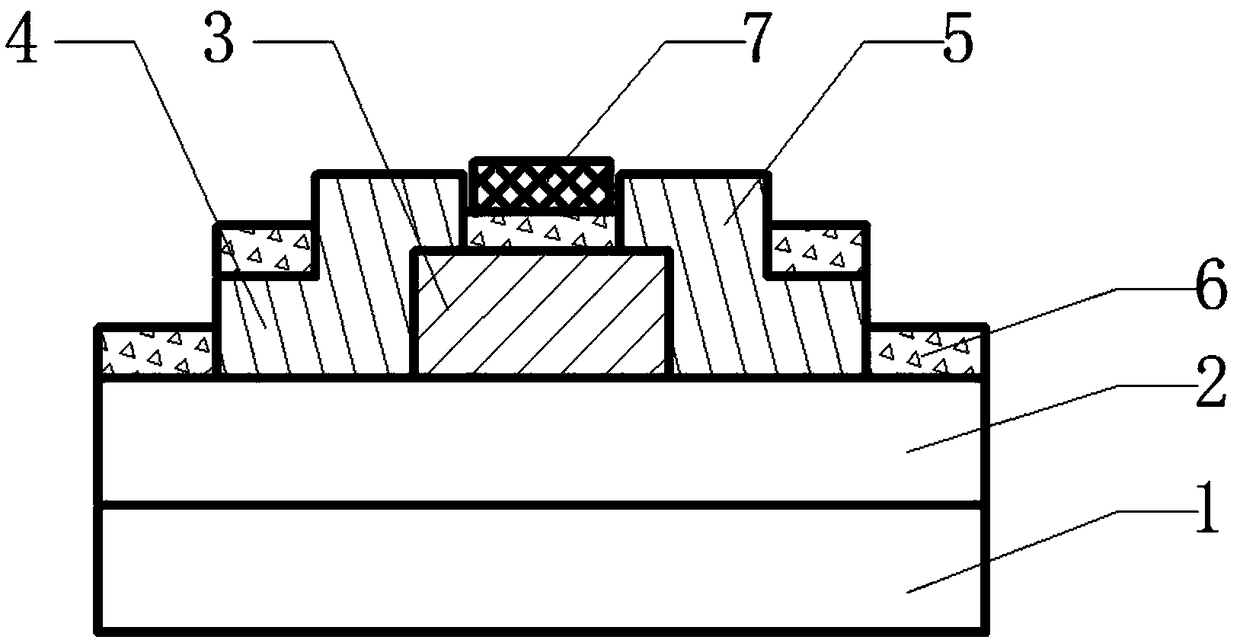
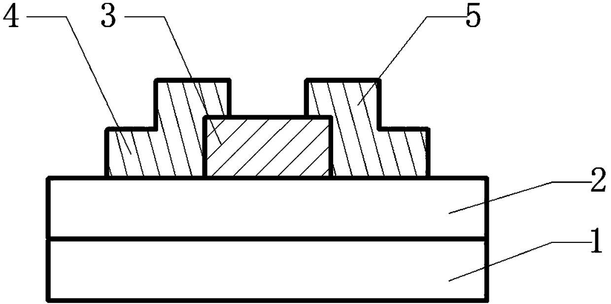
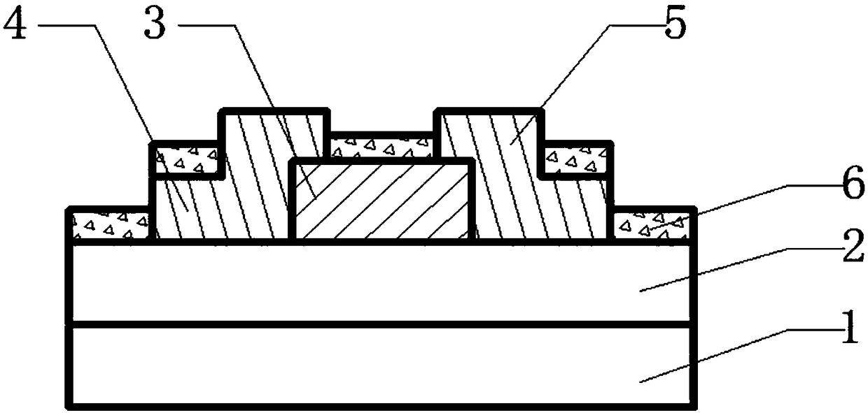
[0033] Step 1: Fabrication of Thin Film Transistors

[0034] Thermally oxidized silicon wafers (SiO) produced by the 46th Research Institute of China Electronics Technology Group Corporation 2 / p+Si(100)) as the substrate, the gate is highly doped p-type Si, the thickness is 375±15um, and the gate dielectric layer is SiO 2 , with a thickness of 100±20nm.

[0035] Use high-temperature tape to attach a mask plate with a width-to-length ratio of 800um:200um on the surface of the gate dielectric, and deposit a semiconductor channel layer in a magnetron sputtering apparatus. The target used is an indium gallium zinc oxide target (IGZO target, In 2 o 3 : Ga 2 o 3 :ZnO=1:1:1), the temperature is controlled at room temperature, the sputtering power is 60W, the...

Embodiment 1

[0049] (1) Preparation of IGZO thin film transistors

[0050] (1.1) Thermally oxidized silicon wafers (SiO 2 / p+Si(100)) as the substrate, the gate is highly doped p-type Si, the thickness is 375±15um, and the gate dielectric layer is SiO 2 , with a thickness of 100±20nm. Use high-temperature tape to attach a mask plate with a width-to-length ratio of 800um:200um on the surface of the gate dielectric, and deposit a semiconductor channel layer in a magnetron sputtering apparatus. The temperature is controlled at room temperature, the sputtering power is 60W, and the sputtering time is It takes about 25 minutes. During the sputtering process, the flow ratio of argon and oxygen into the chamber of the magnetron sputtering instrument is 6sccm:0sccm, the gas pressure in the chamber is 0.19pa, and the thickness of the deposited semiconductor channel layer is approximately 45nm.

[0051] (1.2) After the semiconductor channel layer is deposited, the source electrode and the drain el...

Embodiment 2

[0062] Example 2 adopts the same preparation process as Example 1, except that the deposited thickness is 8nm when electron beam evaporation is used to prepare the tin oxide thin film, that is, the covering layer.


PUM


Abstract

The invention discloses a thin film transistor structured visible blind photoelectric detector. The thin film transistor structured visible blind photoelectric detector comprises a thin film transistor, wherein the thin film transistor comprises a gate, a semiconductor channel and a gate dielectric layer, the gate dielectric layer is arranged between the gate and the semiconductor channel, the thin film transistor structured visible blind photoelectric detector also comprises a layer of transparent complementary type semiconductor thin film and a transparent metal oxide thin film, the complementary type semiconductor thin film is arranged at one side, far away from the gate dielectric layer, of the semiconductor channel layer and is suitably used for forming a pn junction with the semiconductor channel layer, and the metal oxide thin film is arranged between the semiconductor channel layer and the complementary type semiconductor thin film. The invention also discloses a fabrication method of the thin film transistor structured visible blind photoelectric detector. The pn junction formed from the complementary type semiconductor thin film and the semiconductor channel layer can generate a built-in electric field to prevent recombination of photo-induced electrons and photo-induced holes, the service lifetime of a photo-induced carrier is prolonged, and the suppression ratio of ultraviolet visible light is increased.

Description

technical field [0001] The application relates to a visible blind photodetector with a thin film transistor structure and a preparation method thereof, belonging to the technical field of semiconductor photoelectric detection. Background technique [0002] Ultraviolet detection technology is a new detection technology developed after infrared detection technology, which is widely used in military, medical, biological, food safety and other fields. The key to ultraviolet detection technology is to prepare ultraviolet photodetectors with high sensitivity, low noise and low power consumption. At present, the ultraviolet photodetector devices that are gradually put into military application and commercialization include ultraviolet photomultiplier tubes, ultraviolet intensifiers and solid-state ultraviolet detectors. Solid-state ultraviolet detectors have always been a research hotspot in various countries. Solid-state ultraviolet detectors are a new type of ultraviolet detect...

Claims


Application Information

Patent Timeline
Patent Type & Authority Patents(China)
IPC IPC(8): H01L31/112H01L31/18
CPCH01L31/112H01L31/18Y02P70/50
Inventor 曹鸿涛余静静梁凌燕张莉莉吴卫华梁玉宋安然
Owner NINGBO INST OF MATERIALS TECH & ENG CHINESE ACADEMY OF SCI
Why Eureka
Try Eureka